BD9415FS
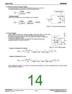
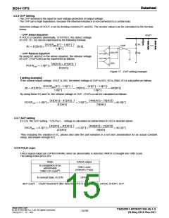
3.2.6 OVP Setting
The OVP terminal is the input for over-voltage protection of output voltage.
The OVP pin is high impedance, because the internal resistance is not connected to a certain bias.
Detection voltage of VOUT is set by dividing resistors R1 and R2. The resistor values can be calculated by the formula
below.
○ OVP Detect Equation
VOUT
If VOUT is boosted abnormally, VOVPDET, the detect voltage
of OVP, R1, R2 can be expressed by the following formula.
R1
R2
VOVPDET [V] 3.0[V]
[k]ꢀ
OVP
R1 R2[k]
+
-
3.0[V]
3.0V/2.9V
○ OVP Release Equation
By using R1 and R2 in the above equation, the release voltage
of OVP, VOVPCAN can be expressed as follows.
OVP COMP
SCP COMP
-
+
0.2V
R1[k] R2[k]
R2[k]
ꢀ
VOVP 2.9[V]
CAN
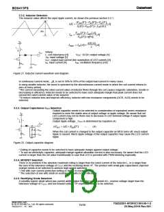
Figure 17 . OVP setting example
【setting example】
If the normal output voltage, VOUT is 58V, the detect voltage of OVP is 63V, R2 is 20kΩ, R1 is calculated as follows.
VOVPDET [V] 3.0[V]
63[V] 3.0[V]
R1 R2[k]
20[k]ꢀ
400[k]
3.0[V]
3.0[V]
By using these R1 and R2, the release voltage of OVP, VOVPCAN can be calculated as follows.
R1[k] R2[k]
R2[k]
400[k] 20[k]
VOVP 2.9[V]
ꢀ 2.9[V]
60.9[V]
CAN
20[k]
3.2.7 SCP setting
【3.2.6) The SCP setting「VSCPDET」 voltage is calculated as below when R1,R2 is decided above:
R1[k] R2[k]
400[k] 20[k]
VSCPDET 0.2[V]
ꢀ 0.2[V]
40.2[V]
R2[k]
20[k]
*Also including the variation in IC, please also take the part variation in a set into consideration for an actual constant
setup, and inquire enough to it.
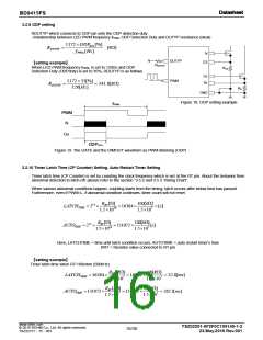
3.2.8 FAILB Logic
FAILB signal output pin (OPEN DRAIN); when an abnormality is detected, NMOS is brought into GND Level.
The rating of this pin is 20V.
State
FAILB output
In completion of an
abnormality
GND Level
(500ohm (Typ))
(After CP count※)
In normal state, In STB
OPEN
※CP count : Count movement after detection of D-S SHORT, LED_OPEN, SHORT, SCP.
www.rohm.com
TSZ02201-0F2F0C100140-1-2
23.May.2016 Rev.001
© 2015 ROHM Co., Ltd. All rights reserved.
15/30
TSZ22111・15・001

 ROHM [ ROHM ]