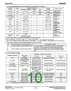
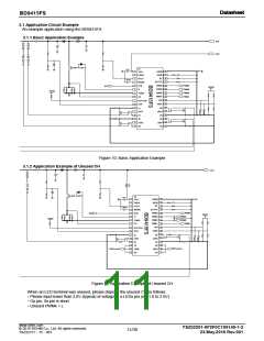
BD9415FS
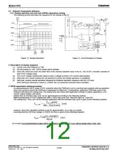
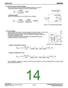
3.2.4 DCDC Oscillation Frequency Setting
RRT which connects to RT pin sets the oscillation frequency fSW of DCDC.
○Relationship between frequency fSW and RT resistance (ideal)
Frequency(fsw)
15000
RRT
[k]ꢀ
fSW [kHz]
【setting example】
When DCDC frequency fSW is set to 200kHz, RRT is as follows.
GATE
CS
RT
Rcs
RRT
15000
15000
GND
RRT
75[k]ꢀ
fSW [kHz] 200[kHz]
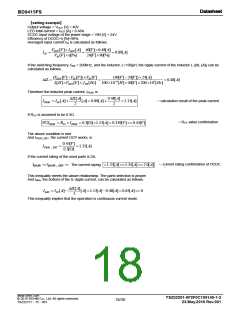
Figure 15. RT terminal setting example
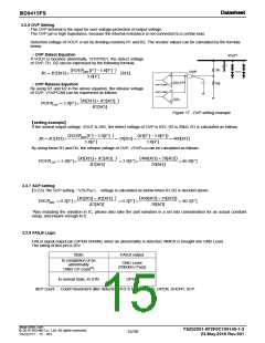
Vin
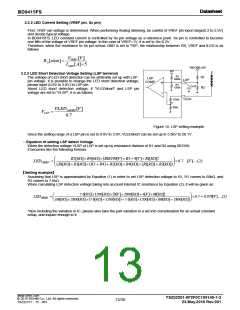
3.2.5 UVLO Setting
Under Voltage Lockout pin is the input voltage of the power stage. IC starts boost
operation if UVLO is more than 2.5V(Typ) and stops if lower than 2.4V(Typ).
Since internal impedance exists in UVLO pin, cautions are needed for selection of
resistance for resistance division.
Vin detection voltage level can be calculated by the following formula using
resistance division of R1 and R2 (unit: kΩ).
R1
R2
Zin=610kΩ
(typ.)
UVLO
1400k
530k
480k
1000pF
AGND AGND
125k
Figure 16. UVLO setting example
○ Equation of Setting UVLO Release
R1 R2
1
1
VinDET 2.5
R1 [V]ꢀ
R2
1400k 125k 530k 480k
○ Equation of Setting UVLO Lock
R1 R2
1
1
Vinlock 2.4
R1 [V]ꢀ
R2
1400k 125k 530k 480k 40k
*Also including the variation in IC, please also take the part variation in a set into consideration for an actual constant
setup, and inquire enough to it.
www.rohm.com
TSZ02201-0F2F0C100140-1-2
23.May.2016 Rev.001
© 2015 ROHM Co., Ltd. All rights reserved.
14/30
TSZ22111・15・001

 ROHM [ ROHM ]