Daattaasshheeeett
BD7xxL5FP-C
●Operational Notes
1) Absolute maximum ratings
Exceeding the absolute maximum rating for supply voltage, operating temperature or other parameters can result in
damages to or destruction of the chip. In this event it also becomes impossible to determine the cause of the damage
(e.g. short circuit, open circuit, etc). Therefore, if any special mode is being considered with values expected to exceed
the absolute maximum ratings, implementing physical safety measures, such as adding fuses, should be considered.
2) The electrical characteristics given in this specification may be influenced by conditions such as temperature, supply
voltage and external components. Transient characteristics should be sufficiently verified.
3) GND electric potential
Keep the GND pin potential at the lowest (minimum) level under any operating condition. Furthermore, ensure that,
including the transient, none of the pin’s voltages are less than the GND pin voltage.
4) GND wiring pattern
When both a small-signal GND and a high current GND are present, single-point grounding (at the set standard point) is
recommended. This in order to separate the small-signal and high current patterns and to ensure that voltage changes
stemming from the wiring resistance and high current do not cause any voltage change in the small-signal GND. Similarly,
care must be taken to avoid wiring pattern fluctuations in any connected external component GND.
5) Inter-pin shorting and mounting errors
Ensure that when mounting the IC on the PCB the direction and position are correct. Incorrect mounting may result in
damaging the IC. Also, shorts caused by dust entering between the output, input and GND pin may result in damaging
the IC.
6) Inspection using the set board
The IC needs to be discharged after each inspection process as, while using the set board for inspection, connecting a
capacitor to a low-impedance pin may cause stress to the IC. As a protection from static electricity, ensure that the
assembly setup is grounded and take sufficient caution with transportation and storage. Also, make sure to turn off the
power supply when connecting and disconnecting the inspection equipment.
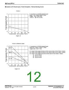
7) Power dissipation (Pd)
Should by any chance the power dissipation rating be exceeded the rise in temperature of the chip may result in
deterioration of the properties of the chip. The absolute maximum rating of the Pd stated in this specification is when the
IC is mounted on a 70mm X 70mm X 1.6mm glass epoxy board. In case of exceeding this absolute maximum rating,
increase the board size and copper area to prevent exceeding the Pd rating.
8) Thermal design
The power dissipation under actual operating conditions should be taken into consideration and a sufficient margin
should be allowed for in the thermal design. On the reverse side of the package this product has an exposed heat pad for
improving the heat dissipation. Use both the front and reverse side of the PCB to increase the heat dissipation pattern as
far as possible. The amount of heat generated depends on the voltage difference across the input and output, load
current, and bias current. Therefore, when actually using the chip, ensure that the generated heat does not exceed the
Pd rating.
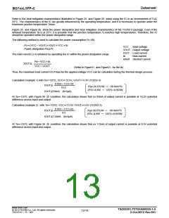
Tjmax: maximum junction temperature=150℃, Ta: ambient temperature (℃), θja: junction-to-ambient thermal
resistance (℃/W), Pd: power dissipation rating (W), Pc: power consumption (W), VCC: input voltage,
VOUT: output voltage, IOUT: load current, Ib: bias current
Power dissipation rating
Power consumption
Pd (W)=(Tjmax-Ta) / θja
Pc (W)=(VCC-VOUT)×IOUT+VCC×Ib
www.rohm.com
TSZ02201-T2T0AN00020-1-2
2.Oct.2012 Rev.001
© 2012 ROHM Co., Ltd. All rights reserved.
15/18
TSZ22111・15・001

 ROHM [ ROHM ]