Daattaasshheeeett
BD7xxL5FP-C
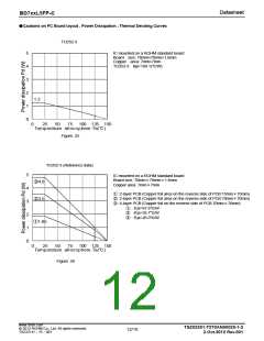
Refer to the heat mitigation characteristics illustrated in Figure 25. and Figure 26. when using the IC in an environment of Ta≧
25°C. The characteristics of the IC are greatly influenced by the operating temperature, and it is necessary to operate under the
maximum junction temperature Timax.
Figure 25. and Figure 26. show the power dissipation and heat mitigation characteristics of the TO252-3 package. Even if the
ambient temperature Ta is at 25°C it is possible that the junction temperature Tj reaches high temperatures. Therefore, the IC
should be operated within the power dissipation range.
The following method is used to calculate the power consumption Pc (W)
Pc=(VCC-VOUT)×IOUT+VCC×Ib
VCC : Input voltage
VOUT : Output voltage
Power dissipation Pd≧Pc
IOUT : Load current
The load current Lo is obtained by operating the IC within the power dissipation range.
Ib
: Bias current
Ishort : Shorted current
Pd-VCC×Ib
VCC-VOUT
IOUT≦
(Refer to Figure11. and Figure21. for the Ib)
Thus, the maximum load current IOUTmax for the applied voltage VCC can be calculated during the thermal design process.
Calculation example 1) with Ta=125℃, VCC=13.5V, VOUT=3.3V (TO252-3)
0.953-13.5×Ib
IOUT≦
θja=26.0℃/W → -38.4mV/℃
10.2
25℃=4.8W → 125℃=0.953W
IOUT≦93mA (Ib:6μA)
At Ta=125℃ with Figure 26 ③ condition, the calculation shows that ca 93mA of output current is possible at 10.2V potential
difference across input and output.
Calculation example 2)with Ta=125℃, VCC=13.5V, VOUT=5.0V (TO252-3)
0.953-13.5×Ib
θja=26.0℃/W → -38.4mV/℃
25℃=4.8W → 125℃=0.953W
IOUT≦
8.5
IOUT≦112mA (Ib:6μA)
At Ta=125℃ with Figure 26 ③ condition, the calculation shows that ca 112mA of output current is possible at 8.5V potential
difference across input and output.
www.rohm.com
TSZ02201-T2T0AN00020-1-2
2.Oct.2012 Rev.001
© 2012 ROHM Co., Ltd. All rights reserved.
13/18
TSZ22111・15・001

 ROHM [ ROHM ]