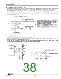
Rx5C348A/B
ꢀ Alarm and Periodic Interrupt
The Rx5C348A/B incorporates the alarm interrupt circuit and the periodic interrupt circuit that are configured to
generate alarm signals and periodic interrupt signals for output from the /INTR pin as described below.
(1) Alarm Interrupt Circuit
The alarm interrupt circuit is configured to generate alarm signals for output from the /INTR, which is driven low
(enabled) upon the occurrence of a match between current time read by the time counters (the day-of-week,
hour, and minute counters) and alarm time preset by the alarm registers (the Alarm_W registers intended for the
day-of-week, hour, and minute digit settings and the Alarm_D registers intended for the hour and minute digit
settings).
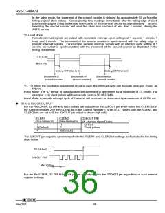
(2) Periodic Interrupt Circuit
The periodic interrupt circuit is configured to generate either clock pulses in the pulse mode or interrupt signals in
the level mode for output from the /INTR pin depending on the CT2, CT1, and CT0 bit settings in the control
register 1.
The above two types of interrupt signals are monitored by the flag bits (i.e. the WAFG, DAFG, and CTFG bits in
the Control Register 2) and enabled or disabled by the enable bits (i.e. the WALE, DALE, CT2, CT1, and CT0
bits in the Control Register 1) as listed in the table below.
Flag bits
Enable bits
Alarm_W
WAFG
WALE
(D1 at Address Fh)
(D7 at Address Eh)
Alarm_D
DAFG
DALE
(D0 at Address Fh)
CTFG
(D6 at Address Eh)
CT2=CT1=CT0=0
Peridic interrupt
(D2 at Address Fh)
(These bit setting of “0” disable the Periodic Interrupt)
(D2 to D0 at Address Eh)
*
*
At power-on, when the WALE, DALE, CT2, CT1, and CT0 bits are set to 0 in the Control Register 1,
the /INTR pin is driven high (disabled).
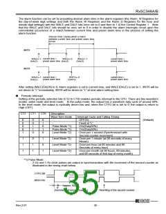
When two types of interrupt signals are output simultaneously from the /INTR pin, the output from the
/INTR pin becomes an OR waveform of their negative logic.
Example: Combined Output to /INTR Pin Under Control of
/ALARM_D and Periodic Interrupt
/Alarm_D
Periodic Interrupt
/INTR
In this event, which type of interrupt signal is output from the /INTR pin can be confirmed by reading the
DAFG, and CTFG bit settings in the Control Register 2.
ꢁ
Alarm Interrupt
The alarm interrupt circuit is controlled by the enable bits (i.e. the WALE and DALE bits in the Control Register 1)
and the flag bits (i.e. the WAFG and DAFG bits in the Control Register 2). The enable bits can be used to
enable this circuit when set to 1 and to disable it when set to 0. When intended for reading, the flag bits can be
used to monitor alarm interrupt signals. When intended for writing, the flag bits will cause no event when set to
1 and will drive high (disable) the alarm interrupt circuit when set to 0.
The enable bits will not be affected even when the flag bits are set to 0. In this event, therefore, the alarm
interrupt circuit will continue to function until it is driven low (enabled) upon the next occurrence of a match
between current time and preset alarm time.
12345
Rev.2.01
- 34 -

 RICOH [ RICOH ELECTRONICS DEVICES DIVISION ]