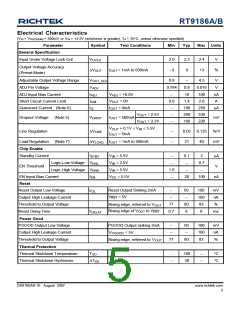
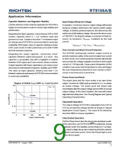
RT9186A/B
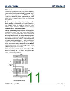
PCB Layout
Good board layout practices must be used or instability
can beinduced because of ground loops and voltage drops.
The input and output capacitors MUST be directly
connected to the input, output, and ground pins of the
device using traces which have no other currents flowing
through them.
The best way to do this is to layout CIN and COUT near the
device with short traces to theVIN, VOUT, and ground pins.
The regulator ground pin should be connected to the
external circuit ground so that the regulator and its
capacitors have a “single point ground”.
It should be noted that stability problems have been seen
in applications where “vias” to an internal ground plane
were used at the ground points of the device and the input
and output capacitors. This was caused by varying ground
potentials at these nodes resulting from current flowing
through the ground plane. Using a single point ground
technique for the regulator and it’ s capacitors fixed the
problem. Since high current flows through the traces going
intoVIN andcoming fromVOUT, Kelvin connect the capacitor
leads to these pins so there is no voltage drop in series
with the input and output capacitors.
Optimum performance can only be achieved when the
device is mounted on a PC board according to the
MSOP-8 Board Layout diagram.
GND
SET
+
V
OUT
PGOOD
/ RST
EN
V
IN
+
GND
MSOP-8 Board Layout
DS9186AB-10 August 2007
www.richtek.com
11

 RICHTEK [ RICHTEK TECHNOLOGY CORPORATION ]