RT8841
After determining desired phase margin, according to the
following Equation :
F
P
= F = F
P1 P2
F
F
F
Z
F
CO
⎛
⎜
⎝
⎞
⎟
⎠
⎛
⎜
⎝
⎞
⎟
⎠
P.M.
2
D
+ 45
tan-1
and
− tan-1
≥
CO
Z
F = F = F
Z2
2
Z
Z1
F
CO
F =
P
F
Z
FZ and FP can be determined by choosing proper FCO to
FZratio to meet Equation (25).Again, R1 can be determined
by the Equation (16).
Frequency (Hz)
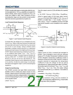
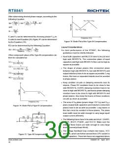
Figure 16. Bode Plot of the Type-III Compensation
R2 can be determined by the following Equation :
Layout Considerations
2
VP
IN(MAX)
F
F
LC
FZ
FCO
⎛
⎜
⎝
⎞
⎟
⎠
CO
R2 = R1×
×
×
For best performance of the RT8841, the following
guidelines must be strictly followed :
V
Other component values of the Type-III compensation can
then be calculated as :
` Input bulk capacitors and MLCCS have to be put near
high side MOSFETs. The connection plane of input
capacitors and high side MOSFETs then can be kept as
square as possible.
1
C1=
2π ×R2×FZ
1
C2 =
1
C1
` The shape of phase planes (the connection plane
between high side MOSFETs, low side MOSFETs and
output inductors) have to be as square as possible. Long
traces, thin bars or separated islands must be avoided
in phase planes.
2π ×R2×FP −
1
C3 =
2π ×R1×FZ
1
R3 =
2π ×C3×FP
` Keep snubber circuits or damping elements near its
objects. Phase RC snubbers have to be close to low
side MOSFETs, UGATE damping resistors have to be
close to high side MOSFETs, and boot to phase damping
resistors have to be close to high side MOSFETs and
phase planes. Also keep the traces of these snubbers
circuits as short as possible.
F
Z
F
P
Frequency (Hz)
` The area of VIN plane (power stage 12V VIN) and VOUT
plane (output bulk capacitors and inductors connection
plane) have to be as wide as possible. Long traces or
thin bars must be avoided in these planes. The plane
trace width must be wide enough to carry large input/
output current (40mil/A).
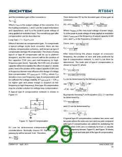
Figure 14. Bode Plot of Type-II Compensation
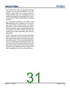
C2
C1
C3
R3
R2
` The following traces have to be wide and short : UGATE,
LGATE, BOOT, PHASE, and VCC12. Make sure the
width of these traces are wide enough to carry large
driving current(at least 40mil).
R1
-
EA
+
+
V
REF
-
` The voltage feedback loop contains two traces, VCC
and VSS, which are Kelvin sensed from CPU socket or
output capacitors. These two traces are suggested above
Figure 15. Type-III Compensation
www.richtek.com
30
DS8841-01 April 2011

 RICHTEK [ RICHTEK TECHNOLOGY CORPORATION ]