RT8841
and the modulator gain of the converter is :
Then determine R2 by the boosted gain of loop gain at
1
VP
crossover :
Fm =
2
F
⎛
⎞
VP
IN(MAX)
ZERO, ESR
FCO
FZERO, ESR
R2 = R1×
×
×
⎜
⎝
⎟
⎠
Where VOUT is the output voltage of the converter, R is
the loading resistance, L and C are the output inductance
and capacitance, and VP is the peak-to-peak voltage of
ramp applied at modulator input. The overall loop gain after
compensation can be described as :
V
F
LC
Where VIN(MAX) is the max input voltage of power stage,
VP is the peak-to-peak voltage of ramp applied at modulator
input, FZERO,ESR is the frequency of output capacitor ESR
zero, and FLC is the frequency of output LC :
Loop Gain = T = Gd x Fm x A
1
FZERO, ESR
=
WhereAdenotes as compensation gain. To compensate
a typical voltage mode buck converter, there are two
ordinary compensation schemes, well known as type-II
compensator and type-III compensator. The choice of using
type-II or type-III compensator will be up to platform
designers, and the main concern will be the position of
the capacitor ESR zero and mid-frequency to high-
frequency gain boost. Typically, the ESR zero of output
capacitor will tend to stabilize the effect of output LC double
poles, hence the positon of the output capacitor ESR zero
in frequency domain may influence the design of voltage
loop compensation. If FZERO,ESR is <1/2FCO where FCO
denotes cross-over frequency, type-II compensation will
be sufficient for voltage stability. If FZERO,ESR is > 1/2FCO
(or higher gain and phase margin is required at mid-
frequency to high-frequency), then type-III compensation
may be a better solution for voltage loop compensation.
2π ×RESR ×C
1
F
LC
=
2π × LC
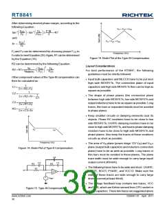
After determining the phase margin at crossover
frequency, the position of zero and pole produced by
type-II compensation network, FZ and FP, can then be
determined. The bode plot of type-II compensation is
shown in Figure14, where
1
FZ =
2π ×R2×C1
1
FP =
2π ×R2×(C1 // C2)
FZ can be determined by the following Equation :
FCO
FZ
FZ
FCO
⎞
⎟
⎠
⎞
⎟
⎠
tan-1 ⎛
− tan-1 ⎛
≥ 90D
⎜
⎜
⎝
⎝
⎛
⎞
FCO
FZERO, ESR
+P.M.− tan-1
⎜
⎝
⎟
⎠
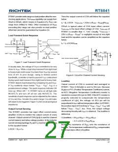
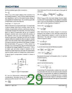
A typical type-II compensation network is shown in
Figure 13.
By properly choosing FZ to fit equation (22), C1 can then
be determined by :
C2
1
C1=
2π ×R2×FZ
C1
R2
and C2 can be determined by :
R1
-
EA
+
1
C2 =
F2
FZ
1
C1
CO
+
2π ×R2×
−
V
REF
-
A typical type-III compensation contains two zeros and
two poles where the extra one zero and one pole compared
with type-II compensation are added for stabilizing the
system when ESR zero is relatively far from LC double
poles in frequency domain. Figure15. and Figure.16 shows
the typical circuit and bode plot of the type-III compensation.
Figure 13. Type-II Compensation
R1 can be determined independently from DC
considerations. Normally choose R1 that the current
passing by will be around 1mA. Therefore,
VREF
1mA
R1=
DS8841-01 April 2011
www.richtek.com
29

 RICHTEK [ RICHTEK TECHNOLOGY CORPORATION ]