RT8841
Current Balance
If the initial current distribution is constant ratio type,
according to Equation(8), reduce RCSN[1] can reduce IL[1]
and improve current balance. If the initial current distribution
is constant difference type, according to Equation(7),
increase RCSP[1] can reduce IL[1] and improve current
balance.
COMP
+
BUF
BUF
PWM[1]
PWM[n]
CMP
RAMP[1]
+
-
-
Interleaved
I
[1] x R
ERR
CB
+
CMP
RAMP[n]
+
-
-
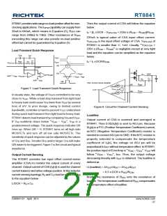
Over Current Protection (OCP)
I
[n] x R
CB
ERR
V
5
CC
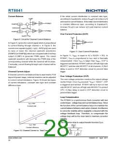
Figure 9. Circuit for Channel Current Balance
ADJ
R1
R2
+
OCP
CMP
In Figure 8, IX[n] is the current signal which is proportional
to current flowing through channel n. In Figure 9, the
current error signals IERR[n] (= IX[n] −AVG(IX[n])) are used
to raise or lower the internal sawtooth waveforms
(RAMP[1] to RAMP[n]) which are compared with ErrorAmp
output (COMP) to generate PWM signal. The raised
sawtooth waveform will decrease the PWM duty of the
corresponding channel while the lowered will increase.
Eventually, current flowing through each channel will be
balanced.
-
IMAX
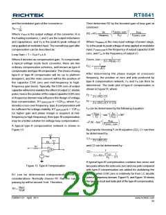
Figure 11. Over Current Protection
In Figure 11, VIMAX is equal to 5V x R2/(R1 + R2). In
RT8841, VADJ is proportional to IOUT and is thermally
compensated. Once VADJ is larger than VIMAX, OCP is
triggered and latched. RT8841 will turn off both high side
MOSFET and low side MOSFET of all channels. A20uS
delay is used in OCP detection circuit to prevent false
trigger.
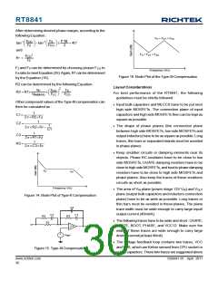
Channel Current Adjust
If channel current is not balanced due to asymmetric PCB
layout of power stage, external resistors can be adjusted
to correct current imbalance. Figure 10 shows two types
of current imbalance, constant ratio type and constant
difference type.
Over Voltage Protectiom (OVP)
The over voltage protection monitors the output voltage
via the FB pin. Once VFB exceeds “VEAP + 150mV”, OVP
is triggered and latched. RT8841 will try to turn on low
side MOSFET and turn off high side MOSFET to protect
CPU. A 20μs delay is used in OVP detection circuit to
prevent false trigger.
I1
Loop Compensation
I2
The RT8841 is a synchronous Buck converter with two
control loops : voltage loop and current balance loop. Since
the function of the current balance loop is to maintain the
current balance between each active channel, its influence
to converter stability will be negligible compared with the
voltage feedback loop. Therefore, to compensate the
voltage loop will be the main task to maintain converter
stability.
I
, total
OUT
Constant ratio
I1
I2
The converter duty-to-output transfer functionGd is :
VOUT
I
, total
OUT
D
Constant difference
Gd =
S
S2
1+
+
Figure 10. Channel Current vs. Total Current
2
L
⎛
⎜
⎝
⎞
⎟
⎠
1
LC
R
C
www.richtek.com
28
DS8841-01 April 2011

 RICHTEK [ RICHTEK TECHNOLOGY CORPORATION ]