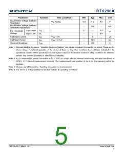
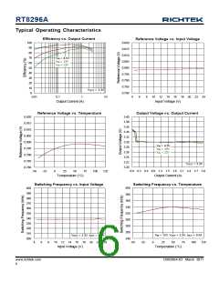
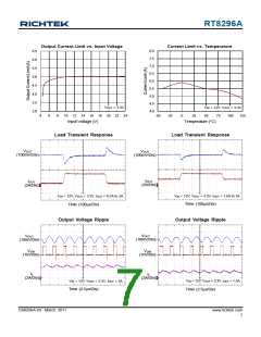
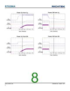
RT8296A
Application Information
The RT8296A is a synchronous high voltage buckconverter
that can support the input voltage range from 4.5V to 23V
and the output current can be up to 3A.
Soft-Start
The RT8296A contains an external soft-start clamp that
gradually raises the output voltage. The soft-start timming
can be programed by the external capacitor between SS
pin andGND. The chip provides a 6mA charge current for
the external capacitor. If 0.1mF capacitor is used to set
the soft-start, it's period will be 13.5ms(typ.).
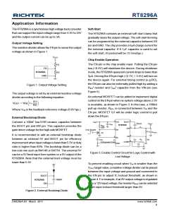
Output Voltage Setting
The resistive divider allows the FB pin to sense the output
voltage as shown in Figure 1.
V
OUT
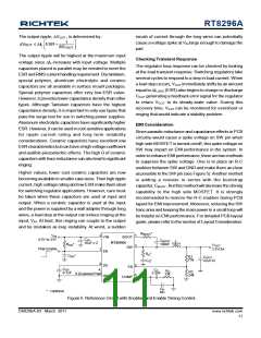
Chip Enable Operation
The EN pin is the chip enable input. Pulling the EN pin
low (<0.4V) will shutdown the device. During shutdown
mode, the RT8296A quiescent current drops to lower than
3mA. Driving the EN pin high (>2.7V, < 5.5V) will turn on
the device again. For external timing control (e.g.RC),
the EN pin can also be externally pulled high by adding a
REN* resistor and CEN* capacitor from the VIN pin (see
Figure 5).
R1
FB
RT8296A
GND
R2
Figure 1. Output Voltage Setting
The output voltage is set by an external resistive voltage
divider according to the following equation :
An external MOSFET can be added to implement digital
control on the EN pin when no system voltage above 2.5V
is available, as shown in Figure 3. In this case, a 100kW
pull-up resistor, REN, is connected between VIN and the
EN pin. MOSFET Q1 will be under logic control to pull
down the EN pin.
R1
R2
æ
è
ö
÷
ø
VOUT = VFB 1+
ç
Where VFB is the feedback reference voltage (0.8V typ.).
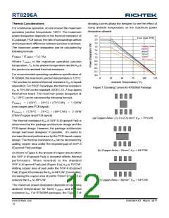
External BootstrapDiode
1
2
BOOT
VIN
V
Connect a 100nF low ESR ceramic capacitor between
the BOOT pin and SW pin. This capacitor provides the
gate driver voltage for the high side MOSFET.
IN
C
BOOT
V
OUT
C
IN
RT8296A
R
100k
EN
L
3
SW
7
Chip Enable
EN
R1
C
OUT
Q1
It is recommended to add an external bootstrap diode
between an external 5V and BOOT pin for efficiency
improvement when input voltage is lower than 5.5V or duty
ratio is higher than 65% .The bootstrap diode can be a
low cost one such as IN4148 or BAT54. The external 5V
can be a 5V fixed input from system or a 5V output of the
RT8296A. Note that the external boot voltage must be
5
6
FB
8
SS
C
R
C
C
R2
C
SS
4,
COMP
9 (Exposed Pad)
GND
C
P
Figure 3. Enable Control Circuit for Logic Control with
Low Voltage
lower than 5.5V
To prevent enabling circuit when VIN is smaller than the
VOUT target value, a resistive voltage divider can be placed
between the input voltage and ground and connected to
the EN pin to adjust IC lockout threshold, as shown in
Figure 4. For example, if an 8V output voltage is regulated
from a 12V input voltage, the resistor REN2 can be selected
to set input lockout threshold larger than 8V.
5V
BOOT
100nF
RT8296A
SW
Figure 2. External BootstrapDiode
DS8296A-03 March 2011
www.richtek.com
9

 RICHTEK [ RICHTEK TECHNOLOGY CORPORATION ]