RT8296A
The output ripple, DVOUT , is determined by :
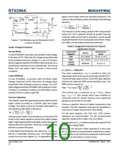
inrush of current through the long wires can potentially
cause a voltage spike at VIN large enough to damage the
part.
é
1
ù
ú
DVOUT £ DIL ESR +
ê
8fCOUT
ë
û
The output ripple will be highest at the maximum input
Checking Transient Response
voltage since DIL increases with input voltage. Multiple
capacitors placed in parallel may be needed to meet the
ESR and RMS current handling requirement.Dry tantalum,
special polymer, aluminum electrolytic and ceramic
capacitors are all available in surface mount packages.
Special polymer capacitors offer very low ESR value.
However, it provides lower capacitance density than other
types. Although Tantalum capacitors have the highest
capacitance density, it is important to only use types that
pass the surge test for use in switching power supplies.
Aluminum electrolytic capacitors have significantly higher
ESR. However, it can be used in cost-sensitive applications
for ripple current rating and long term reliability
considerations. Ceramic capacitors have excellent low
ESR characteristics but can have a high voltage coefficient
and audible piezoelectric effects. The high Q of ceramic
capacitors with trace inductance can also lead to significant
ringing.
The regulator loop response can be checked by looking
at the load transient response. Switching regulators take
several cycles to respond to a step in load current. When
a load step occurs, VOUT immediately shifts by an amount
equal to DILOAD (ESR) also begins to charge or discharge
COUT generating a feedback error signal for the regulator
to return VOUT to its steady-state value. During this
recovery time, VOUT can be monitored for overshoot or
ringing that would indicate a stability problem.
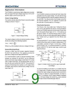
EMI Consideration
Since parasitic inductance and capacitance effects in PCB
circuitry would cause a spike voltage on SW pin when
high side MOSFET is turned-on/off, this spike voltage on
SW may impact on EMI performance in the system. In
order to enhance EMI performance, there are two methods
to suppress the spike voltage. One is to place an R-C
snubber between SW and GND and make them as close
as possible to the SW pin (see Figure 5). Another method
is adding a resistor in series with the bootstrap
capacitor, CBOOT. But this method will decrease the driving
capability to the high side MOSFET. It is strongly
recommended to reserve the R-C snubber during PCB
layout for EMI improvement. Moreover, reducing the SW
trace area and keeping the main power in a small loop will
be helpful on EMI performance. For detailed PCB layout
guide, please refer to the section of Layout Consideration.
Higher values, lower cost ceramic capacitors are now
becoming available in smaller case sizes. Their high ripple
current, high voltage rating and low ESR make them ideal
for switching regulator applications. However, care must
be taken when these capacitors are used at input and
output. When a ceramic capacitor is used at the input
and the power is supplied by a wall adapter through long
wires, a load step at the output can induce ringing at the
input, VIN. At best, this ringing can couple to the output
and be mistaken as loop instability. At worst, a sudden
R
*
BOOT
1
3
2
V
IN
BOOT
RT8296A
VIN
4.5V to 23V
C
IN
10µF x 2
C
100nF
BOOT
L
10µH
R
*
EN
V
OUT
SW
Chip Enable
3.3V/3A
7
EN
R *
S
C
*
EN
R1
75k
C
OUT
22µFx2
C *
S
8
SS
5
6
FB
C
0.1µF
SS
4,
C
C
R
C
R2
24k
3.3nF
9 (Exposed Pad)
13k
GND
COMP
C
P
* : Optional
NC
Figure 5. Reference Circuit with Snubber and Enable Timing Control
DS8296A-03 March 2011
www.richtek.com
11

 RICHTEK [ RICHTEK TECHNOLOGY CORPORATION ]