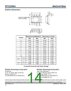
RT8296A
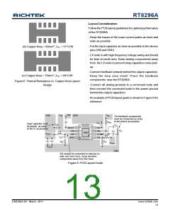
Layout Consideration
Follow the PCB layout guidelines for optimal performance
of the RT8296A.
} Keep the traces of the main current paths as short and
wide as possible.
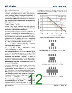
(d) CopperArea = 50mm2 ,qJA = 51°C/W
} Put the input capacitor as close as possible to the device
pins (VIN andGND).
} LX node is with high frequency voltage swing and should
be kept at small area. Keep analog components away
from the LX node to prevent stray capacitive noise pick-
up.
} Connect feedback network behind the output capacitors.
Keep the loop area small. Place the feedback
components near the RT8296A.
(e) CopperArea = 70mm2 ,qJA = 49°C/W
Figure 6. Themal Resistance vs. CopperArea Layout
Design
} Connect all analog grounds to a command node and
then connect the command node to the power ground
behind the output capacitors.
} An example of PCB layout guide is shown in Figure 6 for
reference.
SW
VIN
VIN
GND
GND
The feedback components
must be connected as close
to the device as possible.
REN
CS
Input capacitor must
be placed as close
to the IC as possible.
CIN
CC
8
BOOT
VIN
SS
2
3
4
RC
7
EN
CP
L1
GND
VOUT
6
5
SW
COMP
FB
9
R1
CS*
GND
RS*
R2
VOUT
COUT
GND
SW should be connected to inductor by
wide and short trace. Keep sensitive
components away from this trace.
Figure 8. PCB Layout Guide
DS8296A-03 March 2011
www.richtek.com
13

 RICHTEK [ RICHTEK TECHNOLOGY CORPORATION ]