RT5779A/B
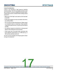
Layout Considerations
Layout is very important in high frequency switching
converter design. The PCB can radiate excessive noise
and contribute to converter instability with improper layout.
Certain points must be considered before starting a layout
using the IC.
Make traces of the high current paths as short and wide
as possible.
Put the input capacitor as close as possible to the device
pins (VINandGND).
The LX node encounters high frequency voltage swings
so it should be kept in a small area. Keep sensitive
components away from the LX node to prevent stray as
possible.
The GND pin should be connected to a strong ground
plane for heat sinking and noise protection.
Avoid using vias in the power path connections that
have switched currents (from CIN to GND and CIN to
VIN) and the switching node (LX).
An TSOT-23-8 (FC)example of PCB layout guide is shown
in Figure 6 for reference.
Copyright 2017 Richtek Technology Corporation. All rights reserved.
©
is a registered trademark of Richtek Technology Corporation.
DS5779A/B-00 October 2017
www.richtek.com
17

 RICHTEK [ RICHTEK TECHNOLOGY CORPORATION ]