RT5779A/B
ΔVOUT_ESR = ΔIOUT x RESR
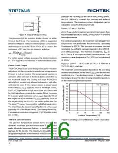
An external MOSFET can be added for the EN pin to be
logic-controlled, as shown in Figure 2. In this case, a
100kΩ pull-up resistor, REN, is connected between VIN
and the ENpin. The MOSFET Q1 will be under logic control
to pull down the EN pin. To prevent the device being
enabled when VIN is smaller than the VOUT target level
or some other desired voltage level, a resistive divider (REN1
and REN2) can be used to externally set the input under-
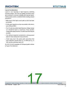
voltage lockout threshold, as shown in Figure 3.
The voltage amplitude (ΔVOUT_SAG) of the capacitive sag
is a function of the load step (ΔIOUT), the output capacitor
value (COUT), the inductor value (L), the input-to-output
voltage differential, and the maximum duty cycle (DMAX).
And, the maximum duty cycle during a fast transient
can be determined by the on-time (tON) and the minimum
off-time (tOFF_MIN) since the ACOTTM control scheme
will ramp the current during on-times, which are spaced
apart by a minimum off-time, that is, as fast as allowed.
The approximate on-time (neglecting parasitics) and
maximum duty cycle for a given input and output voltage
can be calculated according to the following equations :
R
EN
V
EN
RT5779A/B
IN
C
EN
GND
V
OUT
t
=
ON
V f
IN SW
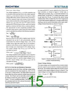
Figure 1. Enable Timing Control
t
ON
D
MAX
=
t
t
OFF_MIN
ON
R
EN
Note the actual on-time will be slightly larger than the
calculated one as the IC will automatically adapt to
compensate the internal voltage drops, such as the
voltage across high-side switch due to on-resistance.
However, both of these can be neglected since the on-
time increase can compensate for the voltage drops.
The output voltage sag (ΔVOUT_SAG) can then be
100k
V
EN
RT5779A/B
GND
IN
Q1
Enable
Figure 2. Logic Control for the EN Pin
calculated as below :
R
EN1
2
V
IN
EN
L(I
)
OUT
V
=
OUT_SAG
2C
V D
V
R
EN2
OUT
IN
MAX OUT
RT5779A/B
GND
The voltage amplitude of the capacitive soar is a function
of the load step (ΔIOUT), the output capacitor value (COUT),
the inductor value (L), and the output voltage (VOUT).
And the output voltage soar (ΔVOUT_SOAR) can be
Figure 3. ResistorDivider for Under-Voltage
Lockout Threshold Setting
calculated as below :
2
L(I
2C
)
OUT
Output Voltage Setting
V
=
OUT_SOAR
V
OUT
OUT
The output voltage can be programmed by a resistive divider
from the output to ground with the midpoint connected to
the FB pin. The resistive divider allows the FB pin to sense
a fraction of the output voltage as shown in Figure 4. The
EN Pin for Start-Up and Shutdown Operation
For automatic start-up, the EN pin, with high-voltage rating,
can be connected to the input supply VIN, either directly
or through a 100kΩ resistor. The large built-in hysteresis
band makes the ENpin useful for simple delay and timing
circuits. The EN pin can be externally connected to VIN
by adding a resistor REN and a capacitor CEN, as shown in
Figure 1, to have an additional delay. The time delay can
be calculated with the EN's internal threshold, at which
switching operation begins.
output voltage is set according to the following equation :
R1
VOUT VTH_FB (1 +
)
R2
where VTH_FB is around 0.6V (Typ).
Copyright 2017 Richtek Technology Corporation. All rights reserved.
©
is a registered trademark of Richtek Technology Corporation.
DS5779A/B-00 October 2017
www.richtek.com
15

 RICHTEK [ RICHTEK TECHNOLOGY CORPORATION ]