RT5779A/B
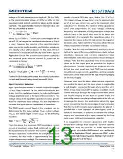
Output Capacitor Selection :
capacitors with ESR of about 5mΩ as output capacitors,
the two output ripple components are as below :
Output capacitance affects the output voltage of the
converter, the response time of the output feedback loop,
and the requirements for output voltage sag and soar. The
sag occurs after a sudden load step current applied, and
the soar occurs after a sudden load removal. Increasing
the output capacitance reduces the output voltage ripple
and output sag and soar, while it increases the response
time that the output voltage feedback loop takes to respond
to step loads, Therefore, there is a tradeoff between output
capacitance and output response. It is recommended to
choose a minimum output capacitance to meet the output
voltage requirements of the converter, and have a quick
transient response to step loads.
VP-P_ESR = IL RESR = 1.294A5m = 6.47mV
IL
1.294A
844μF1500kHz
VP-P_C
=
=
8COUT fSW
ꢀꢀꢀꢀꢀ= 2.451mV
VP-P = VP-P_ESR VP-P_C= 8.921mV
Output Transient Undershoot and Overshoot
In addition to the output voltage ripple at the switching
frequency, the output capacitor and its ESR also affect
output voltage sag, which is undershoot on a positive
load step, and output voltage soar, which is overshoot
on a negative load step. With the built-in ACOTTM
architecture, the IC can have very fast transient
responses to the load steps and small output transients.
The ESR of the output capacitor affects the damping of
the output filter and the transient response. In general,
low-ESR capacitors are good choices due to their
excellent capability in energy storage and transient
performance. The RT5779A/B, therefore, is specially
optimized for ceramic capacitors. Consider also DC bias
and aging effects while selecting the output capacitor.
However, the combination of a small ceramic output
capacitor (that is, of little capacitance) and a low output
voltage (that is, only little charge stored in the output
capacitor), used in low-duty-cycle applications (which
require high inductance to get reasonable ripple currents
for high input voltages), causes an increase in the size
of voltage variations (i.e. sag/soar) in response to very
quick load changes. Typically, the load changes slowly,
compared with the IC's switching frequency. However,
for present-day applications, more and more digital
blocks may exhibit nearly instantaneous large transient
load changes. Therefore, in the following section, how
to calculate the worst-case voltage swings in response
to very fast load steps will be explained in details.
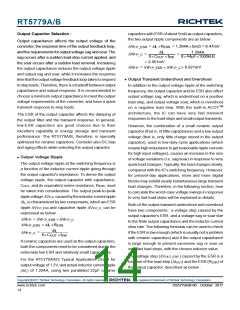
Output Voltage Ripple
The output voltage ripple at the switching frequency is
a function of the inductor current ripple going through
the output capacitor's impedance. To derive the output
voltage ripple, the output capacitor with capacitance,
COUT, and its equivalent series resistance, RESR, must
be taken into consideration. The output peak-to-peak
ripple voltage ΔVP-P, caused by the inductor current ripple
ΔIL, is characterized by two components, which are ESR
ripple ΔVP-P_ESR and capacitive ripple ΔVP-P_C, can be
expressed as below :
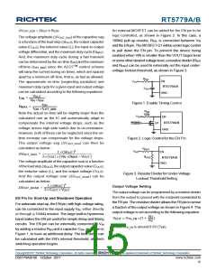
Both of the output transient undershoot and overshoot
have two components : a voltage step caused by the
output capacitor's ESR, and a voltage sag or soar due
to the finite output capacitance and the inductor current
slew rate. The following formulas can be used to check
if the ESR is low enough (which is usually not a problem
with ceramic capacitors) and if the output capacitance
is large enough to prevent excessive sag or soar on
very fast load steps, with the chosen inductor value.
VP-P = VP-P_ESR VP-P_C
VP-P_ESR = IL RESR
IL
VP-P_C
=
8COUT fSW
If ceramic capacitors are used as the output capacitors,
both the components need to be considered due to the
extremely low ESR and relatively small capacitance.
The voltage step (ΔVOUT_ESR ) caused by the ESR is a
function of the load step (ΔIOUT) and the ESR (RESR) of
the output capacitor, described as below :
For the RT5779A/B's Typical Application Circuit for
output voltage of 1.2V, and actual inductor current ripple
(ΔIL) of 1.294A, using two paralleled 22μF ceramic
Copyright 2017 Richtek Technology Corporation. All rights reserved.
©
is a registered trademark of Richtek Technology Corporation.
www.richtek.com
14
DS5779A/B-00 October 2017

 RICHTEK [ RICHTEK TECHNOLOGY CORPORATION ]