RT5779A/B
V
package, the PCB layout, the rate of surrounding airflow,
and the difference between the junction and ambient
temperatures. The maximum power dissipation can be
calculated using the following formula :
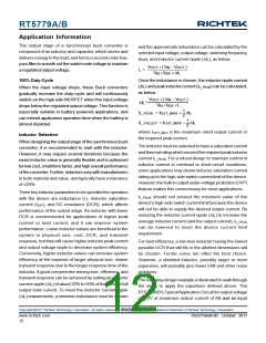
OUT
R1
FB
RT5779A/B
R2
PD(MAX) = (TJ(MAX) − TA) / θJA
GND
where TJ(MAX) is the maximum junction temperature, TA is
the ambient temperature, and θJA is the junction-to-ambient
thermal resistance.
Figure 4. Output Voltage Setting
The placement of the resistive divider should be within
5mm of the FB pin. The resistance of R2 is suggested
between 10kΩ and 100kΩ to minimize power consumption
and noise pick-up at the FB pin. Once R2 is chosen, the
resistance of R1 can then be obtained as below :
For continuous operation, the maximum operating junction
temperature indicated under Recommended Operating
Conditions is 125°C. The junction-to-ambient thermal
resistance, θJA, is highly package dependent. For a TSOT-
23-8 (FC) package, the thermal resistance, θJA, is
68.2°C/W on a four-layer Richtek Evaluation Board. The
maximum power dissipation at TA = 25°C can be calculated
as below :
R2(V
V
)
OUT
TH_FB
R1
V
TH_FB
For better output voltage accuracy, the divider resistors
(R1 and R2) with 1% tolerance or better should be used.
PD(MAX) = (125°C − 25°C) / (68.2°C/W) = 1.46W for a
TSOT-23-8 (FC) package.
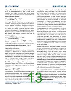
Power-Good Output
The PGOOD pin is an open-drain power-good indication
output and is to be connected to an external voltage source
through a pull-up resistor. The power-good function is
activated after soft-start is finished and is controlled by
the feedback signal VFB. During soft-start, PGOOD is
actively held low and only allowed to transition high after
soft-start is over. If VFB raises above a power-good
threshold (VTH_PGLH) (typically 95% of the target value),
the PGOODpin will be in high impedance and VPGOOD will
be held high after a certain delay elapsed. When VFB drops
by a power-good hysteresis (ΔVTH_PGLH) (typically 5% of
the target value) or exceeds VTH_PGHL (typically 110% of
the target value), the PGOOD pin will be pulled low. For
VFB above VTH_PGHL, VPGOOD will be pulled high again when
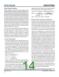
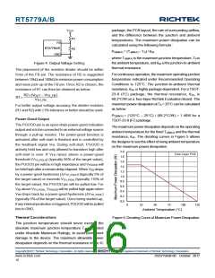
The maximum power dissipation depends on the operating
ambient temperature for the fixed TJ(MAX) and the thermal
resistance, θJA. The derating curves in Figure 5 allows
the designer to see the effect of rising ambient temperature
on the maximum power dissipation.
2.0
Four-Layer PCB
1.8
1.6
1.4
1.2
1.0
0.8
0.6
0.4
0.2
0.0
VFB drops back by a power-good hysteresis (ΔVTH_PGHL
)
(typically 5% of the target value). Once being started-up,
if any internal protection is triggered, PGOODwill be pulled
low to GND.
0
25
50
75
100
125
Ambient Temperature (°C)
Thermal Considerations
Figure 5. Derating Curve of Maximum PowerDissipation
The junction temperature should never exceed the
absolute maximum junction temperature TJ(MAX), listed
under Absolute Maximum Ratings, to avoid permanent
damage to the device. The maximum allowable power
dissipation depends on the thermal resistance of the IC
Copyright 2017 Richtek Technology Corporation. All rights reserved.
©
is a registered trademark of Richtek Technology Corporation.
www.richtek.com
16
DS5779A/B-00 October 2017

 RICHTEK [ RICHTEK TECHNOLOGY CORPORATION ]