RJK0331DPB
Silicon N Channel Power MOS FET
Power Switching
REJ03G1640-0400
Rev.4.00
Apr 10, 2008
Features
•
•
•
•
•
High speed switching
Capable of 4.5 V gate drive
Low drive current
High density mounting
Low on-resistance
RDS(on) = 2.6 mΩ typ. (at VGS = 10 V)
Pb-free
•
Outline
RENESAS Package code: PTZZ0005DA-A
(Package name: LFPAK)
5
D
5
1, 2, 3 Source
4
G
4
5
Gate
Drain
4
3
2
1
S S S
1
2 3
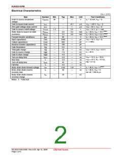
Absolute Maximum Ratings
(Ta = 25°C)
Item
Drain to source voltage
Gate to source voltage
Drain current
Symbol
VDSS
VGSS
ID
Ratings
Unit
30
V
V
±20
40
A
Note1
Drain peak current
ID(pulse)
IDR
160
A
Body-drain diode reverse drain current
Avalanche current
40
A
Note 2
IAP
20
A
Note 2
Avalanche energy
EAR
40
50
mJ
W
Channel dissipation
Pch Note3
θch-C
Tch
Channel to Case Thermal Resistance
Channel temperature
2.5
°C/W
°C
°C
150
Storage temperature
Tstg
–55 to +150
Notes: 1. PW ≤ 10 µs, duty cycle ≤ 1%
2. Value at Tch = 25°C, Rg ≥ 50 Ω
3. Tc = 25°C
REJ03G1640-0400 Rev.4.00 Apr 10, 2008
Page 1 of 6

 RENESAS [ RENESAS TECHNOLOGY CORP ]