R32C/118 Group
1. Overview
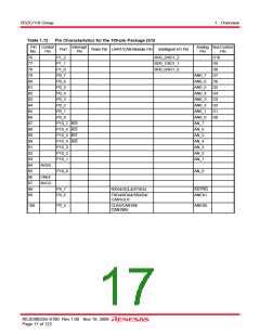
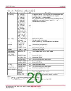
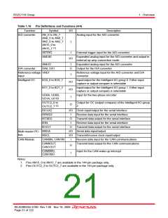
Table 1.16
Function
Pin Definitions and Functions (4/4)
Symbol
I/O
Description
A/D converter
AN_0 to AN_7
AN0_0 to AN0_7
AN2_0 to AN2_7
AN15_0 to
Analog input for the A/D converter
I
(1)
AN15_7
ADTRG
I
External trigger input for the A/D converter
ANEX0
Expanded analog input for the A/D converter and output in
external op-amp connection mode
I/O
ANEX1
I
Expanded analog input for the A/D converter
Output for the D/A converter
D/A converter
DA0, DA1
O
Referencevoltage VREF
input
Reference voltage input for the A/D converter and D/A
converter
I
Intelligent I/O
IIO0_0 to IIO0_7
Input/output for the Intelligent I/O group 0. Either input
capture or output compare is selectable
I/O
I/O
I
IIO1_0 to IIO1_7
Input/output for the Intelligent I/O group 1. Either input
capture or output compare is selectable
UD0A, UD0B,
UD1A, UD1B
Input for the two-phase encoder
OUTC2_0 to
Output for OC (output compare) of the Intelligent I/O group
2
O
(2)
OUTC2_7
ISCLK2
ISRXD2
ISTXD2
IEIN
I/O Clock input/output for the serial interface
I
Receive data input for the serial interface
Transmit data output for the serial interface
Receive data input for the serial interface
Transmit data output for the serial interface
O
I
IEOUT
O
2
MSDA
I/O Serial data input/output
Multi-master I C-
bus
MSCL
I/O Transmit/receive clock input/output
CAN Module
CAN0IN, CAN1IN
I
Receive data input for the CAN communications
Transmit data output for the CAN communications
CAN0OUT,
CAN1OUT
O
CAN0WU,
CAN1WU
Input for the CAN wake-up interrupt
I
Notes:
1. Pins AN15_0 to AN15_7 are available in the 144-pin package only.
2. Pins OUTC2_3 to OUTC2_7 are available in the 144-pin package only.
REJ03B0255-0100 Rev.1.00 Nov 19, 2009
Page 21 of 122

 RENESAS [ RENESAS TECHNOLOGY CORP ]