R32C/118 Group
1. Overview
1.5
Pin Definitions and Functions
Table 1.13 to Table 1.17 show the pin definitions and functions.
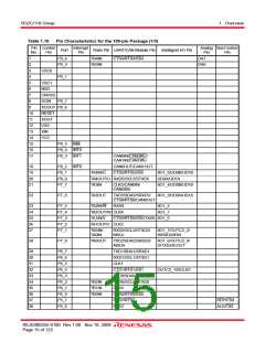
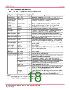
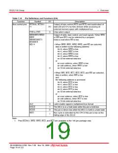
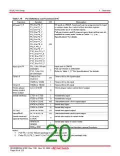
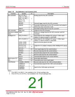
Table 1.13
Function
Power supply
Pin Definitions and Functions (1/4)
Symbol
VCC, VSS
I/O
I
Description
Applicable as follows: VCC = 3.0 to 5.5 V, VSS = 0 V
Connecting pins VDC0, VDC1
for decoupling
A decoupling capacitor for internal voltage should be
connected between VDC0 and VDC1
—
capacitor
Analog power
supply
AVCC, AVSS
Power supply for the A/D converter. AVCC and AVSS
should be connected to VCC and VSS, respectively
I
Reset input
CNVSS
RESET
CNVSS
NSD
I
I
The MCU is reset when this pin is driven low
This pin should be connected to VSS via a resistor
Debug port
This pin is to communicate with a debugger. It should be
connected to VCC via a resistor of 1 to 4.7 kΩ
I/O
Main clock input XIN
Input/output for the main clock oscillator. A crystal, or a
ceramic resonator should be connected between pins XIN
and XOUT. An external clock should be input at the XIN
while leaving the XOUT open
I
Main clock output XOUT
O
I
Sub clock input
XCIN
Input/output for the sub clock oscillator. A crystal oscillator
should be connected between pins XCIN and XCOUT. An
external clock should be input at the XCIN while leaving the
XCOUT open
Sub clock output XCOUT
O
BCLK output
Clock output
BCLK
O
O
BCLK output
CLKOUT
INT0 to INT8
Output of the clock with the same frequency as fC, f8, or f32
Input for external interrupts
(1)
External interrupt
input
I
NMI input
P8_5/NMI
I
I
Input for NMI
Key input interrupt KI0 to KI3
Input for the key input interrupt
Bus control pins D0 to D7
Input/output of data (D0 to D7) while accessing an external
memory space with a separate bus
I/O
I/O
D8 to D15
Input/output of data (D8 to D15) while accessing an
external memory space with 16-bit or 32-bit separate bus
(2)
Input/output of data (D16 to D31) while accessing an
external memory space with 32-bit separate bus
D16 to D31
A0 to A23
I/O
O
Output of address bits A0 to A23
A0/D0 to A7/D7
Output of address bits (A0 to A7) and input/output of data
I/O (D0 to D7) by time-division while accessing an external
memory space with multiplexed bus
A8/D8 to
A15/D15
Output of address bits (A8 to A15) and input/output of data
I/O (D8 to D15) by time-division while accessing an external
memory space with 16-bit or 32-bit multiplexed bus
Notes:
1. Pins INT6 to INT8 are available in the 144-pin package only.
2. Pins D16 to D31 are available in the 144-pin package only.
REJ03B0255-0100 Rev.1.00 Nov 19, 2009
Page 18 of 122

 RENESAS [ RENESAS TECHNOLOGY CORP ]