R32C/118 Group
1. Overview
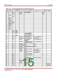
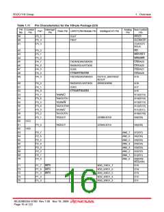
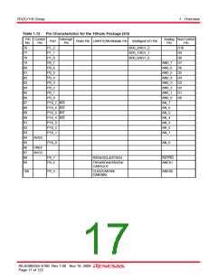
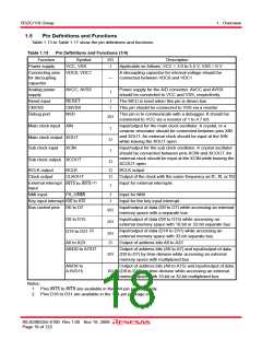
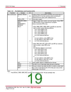
Table 1.14
Pin Definitions and Functions (2/4)
Symbol I/O
Function
Description
Output of byte control (BC0 and BC2) and input/output of
Bus control pins BC0/D0, BC2/D1
(1)
I/O data (D0 and D1) by time-division while accessing an
external memory space with multiplexed bus
CS0 to CS3
O
Chip select output
WR0/WR1/WR2/
WR3
Output of write, byte control, and read signals. Either WRx
or WR and BCx can be selected by a program.
Data is read when RD is low.
WR/BC0/BC1/
BC2/BC3
(1)
• When WR0, WR1, WR2, WR3, and RD are selected,
data is written to the following address:
4n+0, when WR0 is low
RD
4n+1, when WR1 is low
4n+2, when WR2 is low
4n+3, when WR3 is low
on 32-bit external data bus
or
an even address, when WR0 is low
an odd address, when WR1 is low
on 16-bit external data bus
O
• When WR, BC0, BC1, BC2, BC3, and RD are selected,
data is written, when WR is low
and
the following address is accessed:
4n+0, when BC0 is low
4n+1, when BC1 is low
4n+2, when BC2 is low
4n+3, when BC3 is low
on 32-bit external data bus
or
an even address, when BC0 is low
an odd address, when BC1 is low
on 16-bit external data bus
ALE
O
I
Latch enable signal in multiplexed bus format
HOLD
HLDA
RDY
The MCU is in a hold state while this pin is held low
This pin is driven low while the MCU is held in a hold state
O
Bus cycle is extended by the CPU if this pin is low on the
falling edge of the BCLK
I
Note:
1. Pins BC2/D1, WR2, WR3, BC2, and BC3 are available in the 144-pin package only.
REJ03B0255-0100 Rev.1.00 Nov 19, 2009
Page 19 of 122

 RENESAS [ RENESAS TECHNOLOGY CORP ]