R32C/118 Group
1. Overview
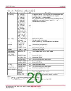
Table 1.15
Pin Definitions and Functions (3/4)
Function
Symbol
I/O
Description
(1, 2)
P0_0 to P0_7
P1_0 to P1_7
P2_0 to P2_7
P3_0 to P3_7
P4_0 to P4_7
P5_0 to P5_7
P6_0 to P6_7
P7_0 to P7_7
P8_0 to P8_4
P8_6, P8_7
I/O ports in CMOS. Each port can be programmed to input
or output under the control of the direction register.
Some ports are 5 V tolerant inputs.
Pull-up resistors and N-channel open drain setting can be
enabled on some ports. Refer to Table 1.17 “Pin
Specifications” for details
I/O port
I/O
P9_0 to P9_7
P10_0 to P10_7
P11_0 to P11_4
P12_0 to P12_7
P13_0 to P13_7
P14_3 to P14_6
P15_0 to P15_7
(2)
P9_1 (for 100-pin
package)
P14_1 (for 144-
pin package)
Input port in CMOS
Pull-up resistor is selectable.
Refer to Table 1.17 “Pin Specifications” for details
Input port
I
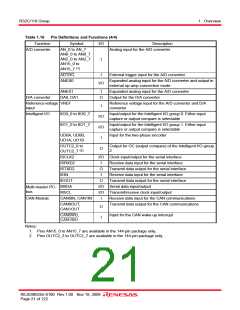
Timer A
Timer B
TA0OUT to
TA4OUT
Timers A0 to A4 input/output
I/O
TA0IN to TA4IN
TB0IN to TB5IN
U,U,V,V,W,W
I
I
Timers A0 to A4 input
Timers B0 to B5 input
Three-phase
motor control
timer output
Three-phase motor control timer output
O
Serial interface
CTS0 to CTS8
RTS0 to RTS8
CLK0 to CLK8
RXD0 to RXD8
TXD0 to TXD8
SDA0 to SDA6
SCL0 to SCL6
STXD0 to
I
Handshake input
Handshake output
O
I/O Transmit/receive clock input/output
I
Serial data input
Serial data output
O
2
I/O Serial data input/output
I C bus
(simplified)
I/O Transmit/receive clock input/output
Serial interface
special functions STXD6
Serial data output in slave mode
O
SRXD0 to
SRXD6
Serial data input in slave mode
I
SS0 to SS6
I
Input to control serial interface special functions
Notes:
1. Port P9_1 in the 100-pin package is an input-only port.
2. Ports P9_0, P9_2, and P11 to P15 are available in the 144-pin package only.
REJ03B0255-0100 Rev.1.00 Nov 19, 2009
Page 20 of 122

 RENESAS [ RENESAS TECHNOLOGY CORP ]