RX62Nグループ、RX621グループ
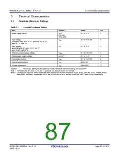
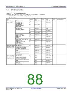
5. Electrical Characteristics
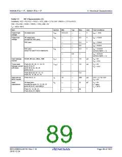
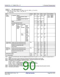
Table 5.4
DC Characteristics (3)
Conditions: VCC = PLLVCC = AVCC = VCC_USB = 2.7 to 3.6V, VREFH = 2.7V to AVCC
VSS = PLLVSS = AVSS = VREFL = VSS_USB = 0V
Ta = -40 to +85C
Item
Symbol
Min.
—
Typ.
—
Max.
100
Unit
mA
Test Conditions
Max.*3
ICC
*4
Supply
current*2
In operation
ICLK = 100MHz
PCLK = 50MHz
BCLK = 50MHz
Peripheral function: Clocks
supplied*5
—
48
—
Peripheral function Clocks not
supplied*5
—
15
—
Sleep
All-module-clock-stop mode*7
—
—
—
—
20
60
28
14
mA
µA
Standby
mode
Software standby mode
0.12
30
3.0
Deep
RTC
RAM,
USB
retained
206
66
software
standby
mode
in
operation
µA
RAM,
USB
—
26
power
supply
halted
µA
µA
RTC
halted
RAM,
USB
retained
—
—
25
21
200
60
RAM,
USB
power
supply
halted
mA
mA
µA
µA
mA
mA
mA
mA
V
Analog power During 12-bit A/D conversion (per unit)
AICC
—
2.5
0.8
0.3
30
3.0
1.2
2.0
35
supply current
During 10-bit A/D conversion (per unit)
—
During D/A conversion (per unit)
Idle (all units)
—
—
Reference
power supply
current
During 12-bit A/D conversion (per unit)
During 10-bit A/D conversion (per unit)
During D/A conversion (per unit)
Idle (all units)
AICC
—
0.5
0.06
0.6
0.4
—
0.7
0.1
1.0
0.6
—
—
—
—
RAM standby voltage
VCC rising gradient
VRAM
2.48
ms/V
SVCC
—
—
20
Note 1. This does not include the pins, which are multiplexed as ports 00 to 02, 07, ports 12, 13, 16, 17, ports 20, 21, and port 33 for 5 V
tolerant.
Note 2. Supply current values are with all output pins unloaded and all input pull-up MOSs in the off state.
Note 3. Measured with clocks supplied to the peripheral functions. This does not include the BGO operation.
Note 4. ICC depends on f (ICLK) as follows. (ICLK: PCLK: BCLK = 8 : 4: 2)
ICC max. = 0.89 x f + 11 (max.)
ICC typ. = 0.43 x f + 5 (normal operation, peripheral function: clocks supplied)
ICC typ. = 0.30 x f + 5 (normal operation, peripheral function: clocks not supplied)
ICC max. = 0.48 x f + 12 (sleep mode)
Note 5. This does not include the BGO operation.
Note 6. Incremented if data is written to or erased from the ROM or data flash for data storage during the program execution.
Note 7. The values are for reference.
R01UH0033JJ0110 Rev.1.10
2010.12.24
Page 90 of 1931

 RENESAS [ RENESAS TECHNOLOGY CORP ]