RX62N Group, RX621 Group
1. Overview
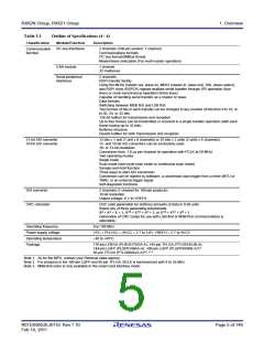
Table 1.1
Outline of Specifications (2 / 4)
Classification
Module/Function
Description
Interrupt
Interrupt control unit
· Peripheral function interrupts: 146 sources
· External interrupts: 16 (pins IRQ0 to IRQ15)
· Non-maskable interrupts: 3 (the NMI pin, oscillation stop detection interrupt, and voltage-
monitoring interrupt)
· Sixteen levels specifiable for the order of priority
User break controller
(as an optional
function)
· Two breakpoint channels
· Address breaks in fetch cycles are specifiable (enabling ROM correction)
External bus extension
· The external address space can be divided into nine areas (CS0 to CS7, SDCS), each
with independent control of access settings.
Capacity of each area: 16 Mbytes (CS0 to CS7), 128 Mbytes (SDCS)
A chip-select signal (CS0# to CS7#, SDCS#) can be output for each area.
Each area is specifiable as an 8-, 16-, or 32-bit bus space (however, only 176-pin
versions support 32-bit bus spaces).
The data arrangement in each area is selectable as little or big endian (only for data).
· SDRAM interface connectable
· Bus format: Separate buses
· Wait control
· Write buffer facility
DMA
DMA controller
· 4 channels
· Three transfer modes: Normal transfer, repeat transfer, and block transfer
· Activation sources: Software trigger, external interrupts, and interrupt requests from
peripheral functions
EXDMA controller
· 2 channels
· Four transfer modes: Normal transfer, repeat transfer, block transfer, and cluster transfer
· Single-address transfer enabled with the EDACK signal
· Capable of direct data transfer to TFT LCD panels
· Activation sources: Software trigger, external DMA requests (EDREQ), and interrupt
requests from peripheral functions
Data transfer
controller
· Three transfer modes: Normal transfer, repeat transfer, and block transfer
· Activation sources: Software trigger, external interrupts and interrupt requests from
peripheral functions
I/O ports
Programmable I/O
ports
· I/O ports for the 176-pin LFBGA/145-pin TFLGA/144-pin LQFP/100-pin LQFP/85-pin
TFLGA
· I/O pins: 126/103/103/72/58
· Input pins: 2/2/2/2/2
· Pull-up resistors: 56/44/44/40/28
· Open-drain outputs: 35/33/33/27/23
· 5-V tolerance: 11/11/11/7/6
Timers
Multi-function timer
pulse unit
· (16 bits x 6 channels) x 2 units
· Time bases for the 12 16-bit timer channels can be provided via up to 32 pulse-input/
output lines and six pulse-input lines
· Select from among eight counter-input clock signals for each channel (PCLK/1, PCLK/4,
PCLK/16, PCLK/64, MTCLKA, MTCLKB, MTCLKC, MTCLKD) other than channel 5, for
which only four signals are available.
· Input capture function
· 21 output compare/input capture registers
· Pulse output mode
· Complementary PWM output mode
· Reset synchronous PWM mode
· Phase-counting mode
· Generation of triggers for A/D converter conversion
Port output enable
· Controls the high-impedance state of the MTU’s waveform output pins
R01DS0052EJ0110 Rev.1.10
Feb 10, 2011
Page 3 of 146

 RENESAS [ RENESAS TECHNOLOGY CORP ]