RX62N Group, RX621 Group
1. Overview
1.
Overview
1.1
Outline of Specifications
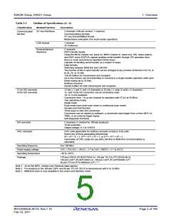
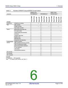
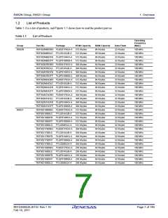
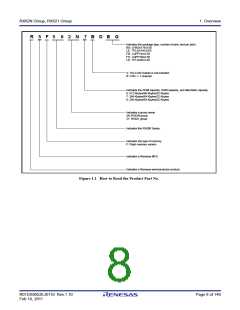
Table 1.1 lists the specifications in outline, and Table 1.2 lists the functions of products.
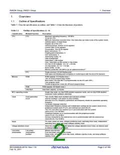
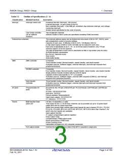
Table 1.1
Outline of Specifications (1 / 4)
Classification
Module/Function
Description
CPU
CPU
· Maximum operating frequency: 100 MHz
· 32-bit RX CPU
· Minimum instruction execution time: One instruction per state (cycle of the system clock)
· Address space: 4-Gbyte linear
· Register set of the CPU
General purpose: Sixteen 32-bit registers
Control: Nine 32-bit registers
Accumulator: One 64-bit register
· Basic instructions: 73
· Floating-point instructions: 8
· DSP instructions: 9
· Addressing modes: 10
· Data arrangement
Instructions: Little endian
Data: Selectable as little endian or big endian
· On-chip 32-bit multiplier: 32 x 32 64 bits
· On-chip divider: 32 / 32 32 bits
· Barrel shifter: 32 bits
· Memory-protection unit (MPU) (as an optional function)*1
FPU
· Single precision (32-bit) floating point
· Data types and floating-point exceptions in conformance with the IEEE754 standard
Memory
ROM
· ROM capacity: 512 Kbytes (max.)
· Two on-board programming modes
Boot mode (The user MAT is programmable via the SCI and USB.)
User program mode
· Parallel programmer mode (for off-board programming)
RAM
RAM capacity: 96 Kbytes (max.)
Data flash
Data flash capacity: 32 Kbytes
MCU operating modes
· Single-chip mode, on-chip ROM enabled expansion mode, and on-chip ROM disabled
expansion mode (software switching)
Clock
Clock generation
circuit
· Two circuits: Main clock oscillator and subclock oscillator
· Internal oscillator: Low-speed on-chip oscillator
· Structure of a PLL frequency synthesizer and frequency divider for selectable operating
frequency
· Oscillation stoppage detection
· Independent frequency-division and multiplication settings for the system clock (ICLK),
peripheral module clock (PCLK), and external bus clock (BCLK)
The CPU and other bus masters run in synchronization with the system
clock (ICLK): 8 to 100 MHz
Peripheral modules run in synchronization with the peripheral module
clock (PCLK): 8 to 50 MHz
· Devices connected to the external bus run in synchronization with the external bus
clock (BCLK): 8 to 50 MHz
Reset
Voltage detection circuit
· Pin reset, power-on reset, voltage-monitoring reset, watchdog timer reset, independent
watchdog timer reset, and deep software standby reset
· When the voltage on VCC falls below the voltage detection level (Vdet), an internal reset
or internal interrupt is generated.
Low power
consumption
Low power
consumption
facilities
· Module stop function
· Four low power consumption modes
Sleep mode, all-module clock stop mode, software standby mode, and deep software
standby mode
R01DS0052EJ0110 Rev.1.10
Feb 10, 2011
Page 2 of 146

 RENESAS [ RENESAS TECHNOLOGY CORP ]