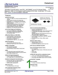
RX62N Group, RX621 Group
1. Overview
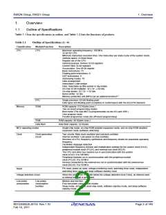
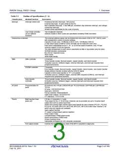
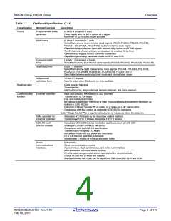
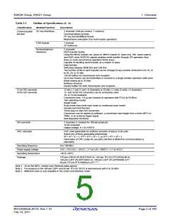
Table 1.1
Outline of Specifications (4 / 4)
Classification
Module/Function
Description
Communication
function
I2C bus interfaces
· 2 channels (100-pin version: 1 channel)
· Communications formats
I2C bus format/SMBus format
Master/slave selectable (For multi-master operation)
CAN module
· 1 channel
· 32 mailboxes
Serial peripheral
interfaces
· 2 channels
· RSPI transfer facility
Using the MOSI (master out, slave in), MISO (master in, slave out), SSL (slave select),
and RSPI clock (RSPCK) signals enables serial transfer through SPI operation (four
lines) or clock-synchronous operation (three lines)
Capable of handling serial transfer as a master or slave
· Data formats
Switching between MSB first and LSB first
The number of bits in each transfer can be changed to any number of bits from 8 to 16, or
to 20, 24, or 32 bits.
128-bit buffers for transmission and reception
Up to four frames can be transmitted or received in a single transfer operation (with each
frame having up to 32 bits)
· Buffered structure
· Double buffers for both transmission and reception
12-bit A/D converter
10-bit A/D converter
· 12 bits x 1 unit (1 unit x 8 channels) or 10 bits x 2 units (2 units x 4 channels);
12- and 10-bit A/D converters can be exclusively used.
· 10- or 12-bit resolution
· Conversion time: 1.0 s per channel (in operation with PCLK at 50 MHz)
· Two operating modes
Single mode
Scan mode (one-cycle scan mode or continuous scan mode)
· Sample-and-hold function
· Three ways to start A/D conversion
Conversion can be started by software, a conversion start trigger from a timer (MTU or
TMR), or an external trigger signal.
· Self-diagnostic functions
D/A converter
CRC calculator
· 2 channels (1 channel for 100-pin products)
· 10-bit resolution
· Output voltage: 0 V to VREFH
· CRC code generation for arbitrary amounts of data in 8-bit units
· Select any of three generating polynomials:
X8 + X2 + X + 1, X16 + X15 + X2 + 1, or X16 + X12 + X5 + 1.
· Generation of CRC codes for use with LSB-first or MSB-first communications is
selectable.
Operating frequency
Power supply voltage
Operating temperature
Package
8 to 100 MHz
VCC = PLLVCC = AVCC = 2.7 to 3.6V, VREFH = 2.7 to AVCC
40 to +85C
176-pin LFBGA (PLBG0176GA-A), 145-pin TFLGA (PTLG0145JB-A),
144-pin LQFP (PLQP0144KA-A), 100-pin LQFP (PLQP0100KB-A)*2
85-pin TFLGA (PTLG0085JA-A)*2,
*
3
Note 1. As for the MPU, contact your Renesas sales agency.
Note 2. For products in the 100-pin LQFP and 85-pin TFLGA, BCLK is synchronized with 8 to 25 MHz.
Note 3. MSB-first order is only available in the smart-card interface mode.
R01DS0052EJ0110 Rev.1.10
Feb 10, 2011
Page 5 of 146

 RENESAS [ RENESAS TECHNOLOGY CORP ]