PDF
最近搜索
热门搜索
发布采购

| 型号: | R5F21134DFP |
| PDF下载: | 下载PDF文件 查看货源 |
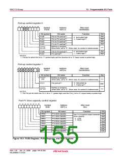
| 内容描述: | 16位单片机M16C族/ R8C / Tiny系列 [16-BIT SINGLE-CHIP MICROCOMPUTER M16C FAMILY/R8C/Tiny SERIES] |
| 分类和应用: | 微控制器和处理器外围集成电路计算机时钟 |
| 文件页数/大小: | 224 页 / 2076 K |
| 品牌: |  RENESAS [ RENESAS TECHNOLOGY CORP ] RENESAS [ RENESAS TECHNOLOGY CORP ] |
专业IC领域供求交易平台:提供全面的IC Datasheet资料和资讯,Datasheet 1000万数据,IC品牌1000多家。