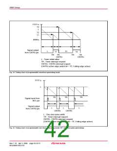
3858 Group
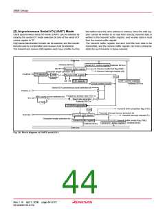
Transmit or receive clock
Transmit buffer write
signal
TBE=0
TSC=0
TBE=1
TBE=0
TBE=1
TSC=1
Serial output TXD
ST
SP
D0
D1
ST
D0
D1
SP
1 start bit
Generated at 2nd bit in 2-stop-bit mode
7 or 8 data bit
1 or 0 parity bit
1 or 2 stop bit (s)
Receive buffer read
signal
RBF=0
RBF=1
SP
RBF=1
SP
ST
Serial input R
X
D
D0
D1
ST
D0
D1
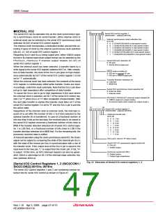
Notes
1: Error flag detection occurs at the same time that the RBF flag becomes “1” (at 1st stop bit, during reception).
2: As the transmit interrupt (TI), when either the TBE or TSC flag becomes “1”, can be selected to occur depending on the setting of the transmit
interrupt source selection bit (TIC) of the serial I/O1 control register.
3: The receive interrupt (RI) is set when the RBF flag becomes “1”.
4: After data is written to the transmit buffer when TSC=1, 0.5 to 1.5 cycles of the data shift cycle is necessary until changing to TSC=0.
Fig. 39 Operation of UART serial I/O1 function
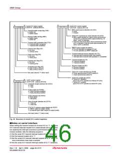
[Serial I/O1 Control Register (SIOCON)] 001A16
The serial I/O1 control register consists of eight control bits for the
serial I/O1 function.
[Transmit Buffer Register/Receive Buffer
Register (TB/RB)] 001816
The transmit buffer register and the receive buffer register are lo-
cated at the same address. The transmit buffer is write-only and
the receive buffer is read-only. If a character bit length is 7 bits, the
MSB of data stored in the receive buffer is “0”.
[UART Control Register (UARTCON)] 001B16
The UART control register consists of four control bits (bits 0 to 3)
which are valid when asynchronous serial I/O is selected and set
the data format of an data transfer and one bit (bit 4) which is al-
ways valid and sets the output structure of the P25/TXD pin.
[Serial I/O1 Status Register (SIOSTS)] 001916
The read-only serial I/O1 status register consists of seven flags
(bits 0 to 6) which indicate the operating status of the serial I/O1
function and various errors.
[Baud Rate Generator (BRG)] 001C16
The baud rate generator determines the baud rate for serial trans-
Three of the flags (bits 4 to 6) are valid only in UART mode.
The receive buffer full flag (bit 1) is cleared to “0” when the receive
buffer register is read.
fer.
The baud rate generator divides the frequency of the count source
by 1/(n + 1), where n is the value written to the baud rate genera-
tor.
If there is an error, it is detected at the same time that data is
transferred from the receive shift register to the receive buffer reg-
ister, and the receive buffer full flag is set. A write to the serial I/O1
status register clears all the error flags OE, PE, FE, and SE (bit 3
to bit 6, respectively). Writing “0” to the serial I/O1 enable bit SIOE
(bit 7 of the serial I/O1 control register) also clears all the status
flags, including the error flags.
Bits 0 to 6 of the serial I/O1 status register are initialized to “0” at
reset, but if the transmit enable bit (bit 4) of the serial I/O1 control
register has been set to “1”, the transmit shift completion flag (bit
2) and the transmit buffer empty flag (bit 0) become “1”.
Rev.1.10 Apr 3, 2006 page 45 of 75
REJ03B0139-0110

 RENESAS [ RENESAS TECHNOLOGY CORP ]