3858 Group
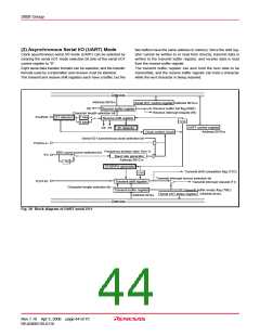
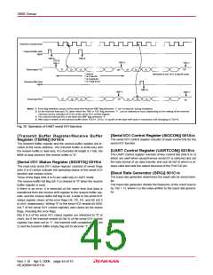
(2) Asynchronous Serial I/O (UART) Mode
Clock asynchronous serial I/O mode (UART) can be selected by
clearing the serial I/O1 mode selection bit (b6) of the serial I/O1
control register to “0”.
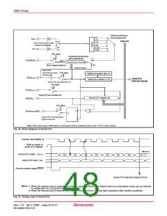
two buffers have the same address in memory. Since the shift reg-
ister cannot be written to or read from directly, transmit data is
written to the transmit buffer register, and receive data is read
from the receive buffer register.
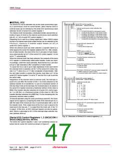
Eight serial data transfer formats can be selected, and the transfer
formats used by a transmitter and receiver must be identical.
The transmit and receive shift registers each have a buffer, but the
The transmit buffer register can also hold the next data to be
transmitted, and the receive buffer register can hold a character
while the next character is being received.
Data bus
Address 001816
Serial I/O1 control register Address 001A16
OE
Character length selection bit
Receive buffer full flag (RBF)
Receive interrupt request (RI)
Receive buffer register
P24/RXD
ST detector
7 bits
8 bits
Receive shift register
1/16
UART control register
PE FE
SP detector
Address 001B16
Clock control circuit
Serial I/O1 synchronous clock selection bit
P26/SCLK1
XIN
Frequency division ratio 1/(n+1)
BRG count source selection bit
1/4
Baud rate generator
Address 001C16
ST/SP/PA generator
1/16
Transmit shift completion flag (TSC)
Transmit interrupt source selection bit
P25/TXD
Transmit shift register
Transmit interrupt request (TI)
Character length selection bit
Transmit buffer register
Address 001816
Transmit buffer empty flag (TBE)
Address 001916
Serial I/O1 status register
Data bus
Fig. 38 Block diagram of UART serial I/O1
Rev.1.10 Apr 3, 2006 page 44 of 75
REJ03B0139-0110

 RENESAS [ RENESAS TECHNOLOGY CORP ]