M37161M8/MA/MF-XXXSP/FP,M37161EFSP/FP
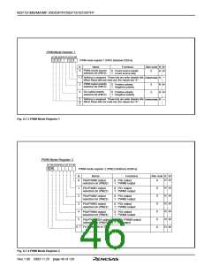
PWM Mode Register 1
b7b6 b5b4b3 b2b1b0
PWM mode register 1 (PM1) [Address 020816
]
After reset
0
B
0
Name
Functions
R W
PWM counts source
selection bit (PM10)
0 : Count source supply
1 : Count source stop
W
R
1, 2
3
—
Nothing is assigned. These bits are write disable bits.
When these bits are read out, the values are “0.”
Indeterminate
0
R
PWM output polarity
selection bit (PM13)
0 : Positive polarity
1 : Negative polarity
R W
R W
4
DA output polarity
selection bit (PM14)
0 : Positive polarity
1 : Negative polarity
0
5
to
7
Nothing is assigned. These bits are write disable bits.
When these bits are read out, the values are “0.”
—
R
Indeterminate
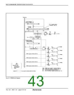
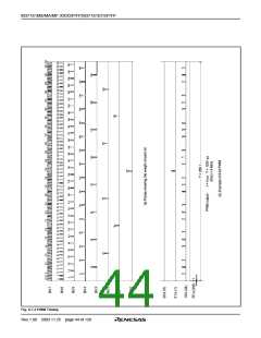
Fig. 8.7.3 PWM Mode Register 1
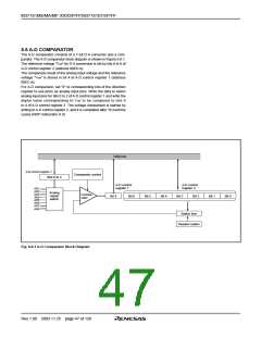
PWM Mode Register 2
b7b6 b5b4b3 b2b1b0
0 0
PWM mode register 2 (PM2) [Address 020916
]
B
0
Name
Functions
0 : P00 output
1 : PWM0 output
After reset R W
0
0
0
0
0
0
0
R W
R W
R W
R W
R W
R W
R W
P0
0
/PWM0 output
selection bit (PM20)
1
P0 /PWM1 output
selection bit (PM21)
1
0 : P0 output
1
2
1 : PWM1 output
2
P0 /PWM2 output
selection bit (PM22)
2
0 : P0 output
1 : PWM2 output
3
3
P0 /PWM3 output
selection bit (PM23)
3
0 : P0 output
1 : PWM3 output
4
4
P0 /PWM4 output
selection bit (PM24)
4
0 : P0 output
1 : PWM4 output
5
P0
0
/PWM0/DA output 0 : P00 PWM0 output
selection bit (PM25)
1 : DA output
6, 7
Fix these bits to “0.”
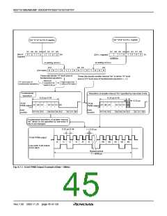
Fig. 8.7.4 PWM Mode Register 2
Rev.1.00 2003.11.25 page 46 of 128

 RENESAS [ RENESAS TECHNOLOGY CORP ]