M37161M8/MA/MF-XXXSP/FP,M37161EFSP/FP
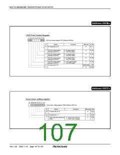
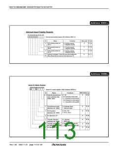
Address 00D116
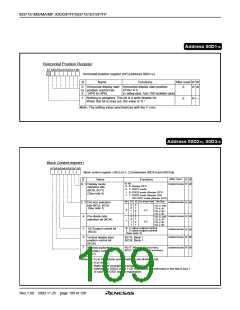
Horizontal Position Register
b7 b6 b5b4 b3 b2b1 b0
Horizontal position register (HP) [Address 00D116
BName Functions
]
After reset R W
0
Horizontal display start position
4Tosc ✕ n
(n: setting value, Tosc: OSD oscillation cycle)
Horizontal display start
to position control bits
0
R W
6
(HP0 to HP6)
Nothing is assigned. This bit is a write disable bit.
When this bit is read out, the value is “0.”
7
0
R —
Note: The setting value synchronizes with the V SYNC
.
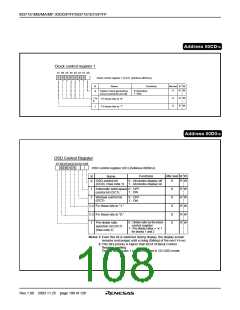
Address 00D216, 00D316
Block Control register i
b7 b6 b5b4 b3 b2b1 b0
Block control register i (BCi) (i=1, 2) [Addresses 00D216 and 00D316
]
After reset
BName
Functions
R W
R W
b1 b0
Indeterminate
0, 1 Display mode
selection bits
(BCi0, BCi1)
0
0
1
1
0: Display OFF
1: OSD1 mode
0: OSD2 mode (Border OFF)
1: OSD2 mode (Border ON)
/CD OSD mode (Border OFF)
(See note 4)
b4 b3 b2 Pre-divide Ratio Dot Size
Indeterminate
Indeterminate
2, 3 Dot size selection
bits (BCi2, BCi3)
(See note 1)
R W
R W
0
0
1
1
0
0
1
1
0
1
0
1
0
1
0
1
1Tc ✕ 1/2H
1Tc ✕ 1H
2Tc ✕ 2H
3Tc ✕ 3H
1Tc ✕ 1/2H
1Tc ✕ 1H
2Tc ✕ 2H
3Tc ✕ 3H
0
1
✕ 2
4
Pre-divide ratio
selection bit (BCi4)
✕ 3
0: 2 value output control
1: 3 value output control
(See note 3)
5
6
OUToutput control bit
(BCi5)
Indeterminate
Indeterminate
R W
R W
Vertical display start
position control bit
(BCi6)
BC16: Block 1
BC26: Block 1
BC17: Window top boundary
BC27: Window bottom boundary
Indeterminate
7
Window top/bottom
boundary control bit
(BCi7)
R W
Notes 1: Tc is OSD clock cycle divided in pre-divide circuit.
2: H is HSYNC
3: Refer to the corresponding figure 8.10.18.
.
4: Selection in OSD2 mode / CD OSD mode is performed in the bits 0 and 1
of color dot OSD control registration.
Rev.1.00 2003.11.25 page 109 of 128

 RENESAS [ RENESAS TECHNOLOGY CORP ]