M37161M8/MA/MF-XXXSP/FP,M37161EFSP/FP
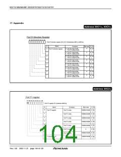
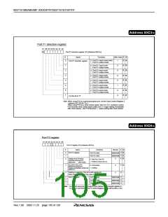
Address 00C316
Port P1 direction register
b7 b6 b5 b4 b3 b2 b1 b0
0
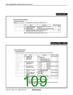
Port P1 direction register (D1) [Address 00C316
]
B
0
Name
Functions
After reset
1
R
R
W
W
0 : Port P1
0
0
input mode (note)
output mode
Port P1 direction register
1 : Port P1
0
0
R
R
W
W
1
2
3
4
5
6
7
0 : Port P1
1 : Port P1
1
1
input mode
output mode
0 : Port P1
1 : Port P1
2
2
input mode
output mode
0 : Port P1
1 : Port P1
3
3
input mode
output mode
0
0
R
R
R
W
W
W
0 : Port P1
1 : Port P1
4
4
input mode
output mode
0 : Port P1
1 : Port P1
5
5
input mode
output mode
1
0
0
0 : Port P1
1 : Port P1
6
6
input mode
output mode
R
R
W
W
Fix this bit to "0"
Note: When using P10 as a general-purpose port, set the Clock Control Register 3
(address 021216) bit 7 to 1.
When using P10 as a clock control signal, refer to 8.14.1 oscillation control.
P10 becomes clock control signal output and H output setting immediately
after reset release , and P16 becomes L output setting after reset release.
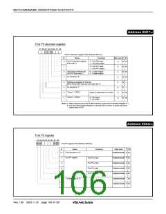
Address 00C616
Port P3 register
b7 b6 b5 b4 b3 b2 b1 b0
Port P3 register (P3) [Address 00C616
]
B
0
1
Name
Functions
data
After reset
Indeterminate
Indeterminate
0
R
R
R
R
W
W
W
W
Port P3 register
Port P3
Port P3
0
1
data
Switch bit of I2C-BUS
interface and port P3
2
0: Port P30, Port P31
1: I2CBUS (SDA3,SCL3)
(BSEL20)
(See note)
SCL3/P3 -SCL1/P1
SDA3/P3 -SDA1/P13
Course connection control bit
(BSEL21)
1
1
3
R
0
W
0: Connection
1: Cutting
0
Nothing is assigned. This bit is write disable bit.
When this bit is read out, the value is "0."
4
0
R
–
5
6
7
Port P3 register
Port P3
Port P3
Port P3
5
6
7
data
data
data
Indeterminate
Indeterminate
Indeterminate
R
R
R
–
–
–
Notes
•
For the ports used as the Multi-master I2C-BUS interface, set their direction registers to 1.
• To use SCL3 and SDA3, set the I2C Control Register (address 00F916) bits 6–7 to 0.
Rev.1.00 2003.11.25 page 105 of 128

 RENESAS [ RENESAS TECHNOLOGY CORP ]