M37161M8/MA/MF-XXXSP/FP,M37161EFSP/FP
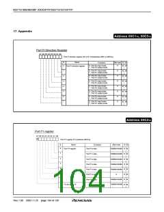
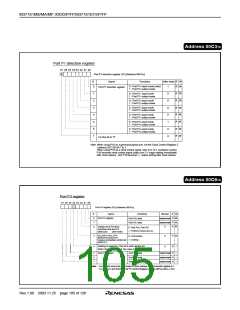
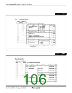
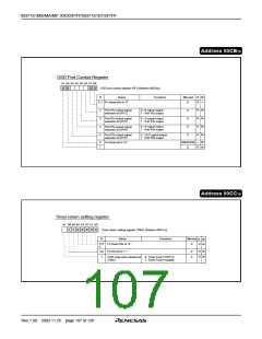
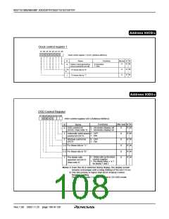
Address 00CD16
Clock control register 1
b7 b6 b5 b4 b3 b2 b1 b0
1
0
0
0
0
0
0
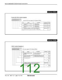
Clock control register 1 (CC1) [Address 00CD16
]
B
0
Name
Functions
0:Operation
After reset
W
R
R
W
W
W
0
System clock generating
circuit control bit (CC10)
1: Stop
0
0
R
R
1 to
6
Fix these bits to "0"
Fix these bits to "1"
7
Address 00D016
OSD Control Register
b7 b6 b5b4 b3 b2b1 b0
0 0 1 1
OSD control register (OC) [Address 00D016
]
Functions
Name
After reset R
W
B
0
OSD control bit
0 : All-blocks display off
0
R W
R W
R W
R W
(OC0) (See note 1) 1 : All-blocks display on
1
2
Automatic solid space 0 : OFF
0
0
0
1 : ON
control bit (OC1)
Window control bit
(OC2)
0 : OFF
1 : ON
3, 4 Fix these bits to “1.”
5, 6 Fix these bits to “0.”
0
0
R W
R W
0 : Divide ratio by the block
control register
1 : Pre-divide ratios = ✕✕1
for blocks 1 and 2
Pre-divide ratio
selection bit (OC7)
(See note 2)
7
Notes 1:Even this bit is switched during display, the display screen
remains unchanged until a rising (falling) of the next VSYNC
2:This bit's priority is higher than BCi4 of Block Control
Register i setting.
The pre-divide ratio 1 cannot be used in CD OSD mode.
Rev.1.00 2003.11.25 page 108 of 128

 RENESAS [ RENESAS TECHNOLOGY CORP ]