M37161M8/MA/MF-XXXSP/FP,M37161EFSP/FP
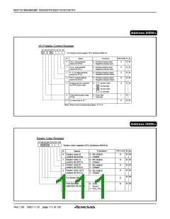
Address 00D816
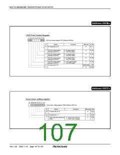
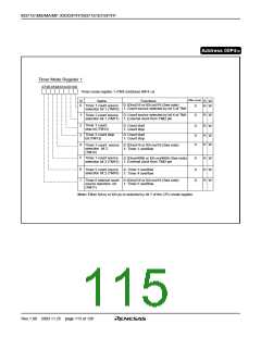
I/O Polarity Control Register
b7 b6 b5 b4 b3 b2 b1 b0
0
0
I/O polarity control register (PC) [Address 00D816
]
After reset
0
B
0
Name
Functions
R
R
W
W
H
SYNC input polarity
switch bit (PC0)
0 : Positive polarity input
1 : Negative polarity input
1
2
3
5
0 : Positive polarity input
1 : Negative polarity input
0
0
0
0
R
R
R
R
W
W
W
W
V
SYNC input polarity
switch bit (PC1)
0 : Positive polarity output
1 : Negative polarity output
R, G, B output polarity
switch bit (PC2)
OUT1 output polarity
switch bit (PC3)
0 : Positive polarity output
1 : Negative polarity output
Display dot line selection
bit (PC5) (See note)
0 : “
” at even field
” at odd field
” at even field
” at odd field
“
1 : “
“
6
Field determination flag
(PC6)
0 : Even field
1 : Odd field
1
0
R
R
—
4, 7
Fix these bits to “0.”
W
Note: Refer to the corresponding figure. 8.10.14.
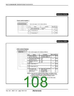
Address 00D916
Raster Color Register
b7 b6 b5b4 b3 b2b1 b0
0 0
0
Raster color register (RC) [Address 00D916
Functions
]
After reset
R
W
B
Name
0 : No output
1 : Output
0
R W
R W
R W
R W
0
1
2
3
Raster color R
control bit (RC0)
Raster color G
control bit (RC1)
0 : No output
1 : Output
0
0
0
Raster color B
control bit (RC2)
0 : No output
1 : Output
Raster color OUT
control bit (RC3)
0 : No output
1 : Output
4
R W
R W
Fix these bits to “0.”
0
0
to
6
7
Port function
selection bit (RC7)
0 : XCIN
,
XCOUT
1 : P26, P27
Rev.1.00 2003.11.25 page 111 of 128

 RENESAS [ RENESAS TECHNOLOGY CORP ]