M37161M8/MA/MF-XXXSP/FP,M37161EFSP/FP
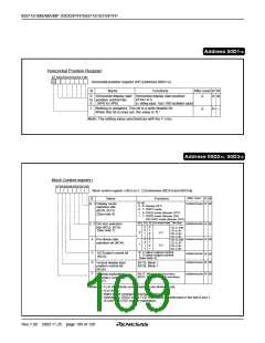
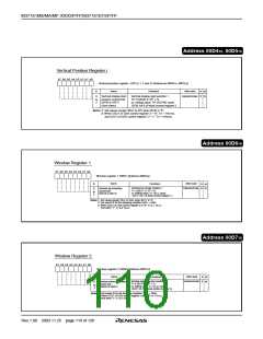
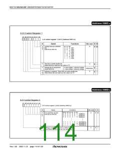
Address 00D416, 00D516
Vertical Position Register i
b7 b6 b5 b4 b3 b2 b1 b0
Vertical position register i (VPi) (i = 1 and 2) [Addresses 00D416, 00D516
]
After reset
Name
B
Functions
R
R
W
W
Vertical display start
position control bits
(VPi0 to VPi7)
Vertical display start position =
TH ✕ (BCi6 ✕ 162 + n)
(n: setting value, TH: HSYNC cycle,
BCi6: bit 6 of block control register i)
Inderterminate
0
to
7
(See notes)
Notes 1: Set values except “0016” to VPi when BCi6 is “0.”
2: When OS21 of OSD control register 2 = “0”, T
H
= 1HSYNC
,
and OS21 of OSD control register 2 = “1”, T
H
= 2HSYNC
.
Address 00D616
Window Register 1
b7 b6 b5 b4 b3 b2 b1 b0
Window register 1 (WN1) [Address 00D616
]
Name
After reset
B
Functions
R
W
W
Window top border position =
✕ (BC17 ✕ 162 + n)
(n: setting value, T : HSYNC cycle,
BC17: bit 7 of block control register 1)
Inderterminate
Window top boundary
control bits
(WN10 to WN17)
R
0
to
7
T
H
H
Notes 1: Set values except “0016” to WN1 when BC17 is “0.”
2: Set values fit for the following condition: WN1 < WN2.
3: When OC21 of OSD control register 2 is “0”, T
And when “1”, T is 2 HSYNC
H is 1 HSYNC.
H
.
Address 00D716
Window Register 2
b7 b6 b5 b4 b3 b2 b1 b0
Window register 2 (WN2) [Address 00D716
]
Name
After reset
B
Functions
R
W
W
Window bottom border position =
TH ✕ (BC27 ✕ 162 + n)
(n: setting value, TH: HSYNC cycle,
Inderterminate
Window bottom boundary
control bits
(WN20 to WN27)
R
0
to
7
BC27: bit 7 of block control register 2)
Notes 1: Set values fit for the following condition: WN1 < WN2.
2: When OC21 of OSD control register 2 is “0”, TH is 1 HSYNC.
And when “1”, TH is 2 HSYNC.
Rev.1.00 2003.11.25 page 110 of 128

 RENESAS [ RENESAS TECHNOLOGY CORP ]