455A Group
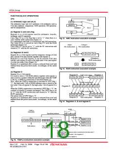
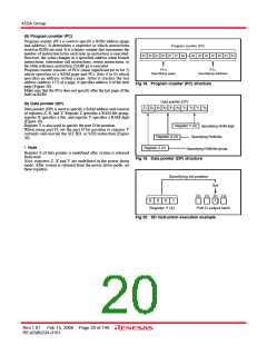
(8) Program counter (PC)
Program counter (PC) is used to specify a ROM address (page
and address). It determines a sequence in which instructions
stored in ROM are read. It is a binary counter that increments the
number of instruction bytes each time an instruction is executed.
However, the value changes to a specified address when branch
instructions, subroutine call instructions, return instructions, or
the table reference instruction (TABP p) is executed.
Program counter consists of PCH (most significant bit to bit 7)
which specifies to a ROM page and PCL (bits 6 to 0) which
specifies an address within a page. After it reaches the last
address (address 127) of a page, it specifies address 0 of the next
page (Figure 18).
Program counter (PC)
p6 p5 p4 p3 p2 p1 p0
a6 a5 a4 a3 a2 a1 a0
PCH
PCL
Specifying page
Specifying address
Fig 18. Program counter (PC) structure
Make sure that the PCH does not specify after the last page of the
built-in ROM.
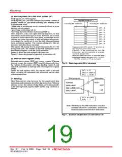
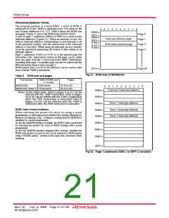
Data pointer (DP)
(9) Data pointer (DP)
Z1 Z0 X3 X2 X1 X0 Y3 Y2 Y1 Y0
Data pointer (DP) is used to specify a RAM address and consists
of registers Z, X, and Y. Register Z specifies a RAM file group,
register X specifies a file, and register Y specifies a RAM digit
(Figure 19).
Register Y is also used to specify the port D bit position.
When using port D, set the port D bit position to register Y
certainly and execute the SD, RD, or SZD instruction (Figure
20).
Register Y (4)
Specifying RAM digit
Specifying RAM file
Register X (4)
• Note
Register Z (2)
Specifying RAM file group
Register Z of data pointer is undefined after system is released
from reset.
Also, registers Z, X and Y are undefined in the power down
mode. After system is returned from the power down mode, set
these registers.
Fig 19. Data pointer (DP) structure
Specifying bit position
Set
D3 D2 D1 D0
1
0
0
0
1
Register Y (4)
Port D output latch
Fig 20. SD instruction execution example
Rev.1.01 Feb 15, 2008 Page 20 of 146
REJ03B0224-0101

 RENESAS [ RENESAS TECHNOLOGY CORP ]