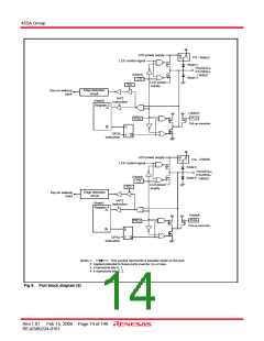
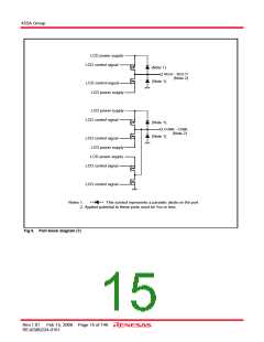
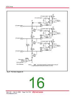
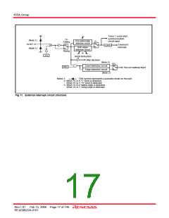
455A Group
FUNCTION BLOCK OPERATIONS
CPU
<Carry>
(1) Arithmetic logic unit (ALU)
(CY)
The arithmetic logic unit ALU performs 4-bit arithmetic such as
4-bit data addition, comparison, AND operation, OR operation,
and bit manipulation.
(M(DP))
Addition
ALU
(2) Register A and carry flag
(A)
<Result>
Register A is a 4-bit register used for arithmetic, transfer,
exchange, and I/O operation.
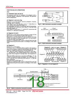
Carry flag CY is a 1-bit flag that is set to “1” when there is a
carry with the AMC instruction (Figure 12).
Fig 12. AMC instruction execution example
It is unchanged with both A n instruction and AM instruction.
The value of A0 is stored in carry flag CY with the RAR
instruction (Figure 13).
<Set>
<Clear>
Carry flag CY can be set to “1” with the SC instruction and
cleared to “0” with the RC instruction.
SC instruction
RC instruction
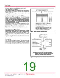
(3) Registers B and E
CY
A0
A3 A2 A1 A0
Register B is a 4-bit register used for temporary storage of 4-bit
data, and for 8-bit data transfer together with register A.
Register E is an 8-bit register. It can be used for 8-bit data
transfer with register B used as the high-order 4 bits and register
A as the low-order 4 bits (Figure 14).
Register E is undefined after system is released from reset and
returned from the power down mode. Accordingly, set the initial
value.
<Rotation>
RAR instruction
CY A3 A2 A1
Fig 13. RAR instruction execution example
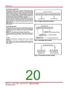
(4) Register D
Register D is a 3-bit register.
Register B
Register A
TAB instruction
It is used to store a 7-bit ROM address together with register A
and is used as a pointer within the specified page when the TABP
p, BLA p, or BMLA p instruction is executed (Figure 15).
Also, when the TABP p instruction is executed at UPTF flag =
“1”, the high-order 2 bits of ROM reference data is stored to the
low-order 2 bits of register D, the high-order 1 bit of register D is
“0”.
B3 B2 B1 B0
A3 A2 A1 A0
TEAB instruction
E7 E6 E5 E4 E3 E2 E1 E0
Register E
When the TABP p instruction is executed at UPTF flag = “0”, the
contents of register D remains unchanged. The UPTF flag is set
to “1” with the SUPT instruction and cleared to “0” with the
RUPT instruction.
TABE instruction
B3 B2 B1 B0
A3 A2 A1 A0
The initial value of UPTF flag is “0”.
Register B
Register A
TBA instruction
Register D is undefined after system is released from reset and
returned from the power down mode. Accordingly, set the initial
value.
Fig 14. Registers A, B and register E
ROM
TABP p
instruction
8
4
0
Specifying address
Low-order 2 bits
PCH
PCL
Register A (4)
Register B (4)
Register D (3)
p6 p5 p4 p3 p2 p1 p0
DR2 DR1 DR0 A3 A2 A1 A0
Middle-order 2 bits
High-order 2 bits
The contents
of register A
Field value p
The contents
of register D
Flag UPTF = 1;
High-order 2 bits of reference data is transferred to the low-order 2
bits of register D.
“0” is stored to the high-order 1 bit of register D.
Flag UPTF = 0;
Data is not transferred to register D.
Fig 15. TABP p instruction execution example
Rev.1.01 Feb 15, 2008 Page 18 of 146
REJ03B0224-0101

 RENESAS [ RENESAS TECHNOLOGY CORP ]