MULTIJUNCTION TIMERS
10.6 TML (Input-Related 32-Bit Timer)
10
10.6.4 TML Control Registers
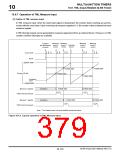
TML0 Control Register (TML0CR)
<Address: H’0080 03EB>
b8
9
10
11
12
13
14
b15
TML0CKS
0
TML0SS0 TML0SS1 TML0SS2 TML0SS3
0
0
0
0
0
0
0
<After reset: H’00>
b
8
Bit Name
TML0SS0
Function
R
R
W
W
0: External input TIN23
1: Input event bus 0
TML0 measure 0 source select bit
9
TML0SS1
0: External input TIN22
1: Input event bus 1
R
R
R
W
W
W
TML0 measure 1 source select bit
10
11
TML0SS2
0: External input TIN21
1: Input event bus 2
TML0 measure 2 source select bit
TML0SS3
0: External input TIN20
1: Input event bus 3
TML0 measure 3 source select bit
12–14
15
No function assigned. Fix to "0".
0
0
TML0CKS (Note 1)
0: BCLK/2
R
W
TML0 clock source select bit
1: Clock bus 1
Note 1: The counter can only be written normally when BCLK/2 is used as the clock source for the counter. If the selected clock
source is not BCLK/2, do not write to the counter because it cannot be written normally.
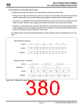
TML1 Control Register (TML1CR)
<Address: H’0080 0FEB>
b8
9
10
11
12
13
14
b15
TML1CKS
0
TML1SS0 TML1SS1 TML1SS2 TML1SS3
0
0
0
0
0
0
0
<After reset: H’00>
b
8
Bit Name
TML1SS0
Function
R
R
W
W
0: External input TIN33
1: Input event bus 0
TML1 measure 0 source select bit
9
TML1SS1
0: External input TIN32
1: Input event bus 1
R
R
R
W
W
W
TML1 measure 1 source select bit
10
11
TML1SS2
0: External input TIN31
1: Input event bus 2
TML1 measure 2 source select bit
TML1SS3
0: External input TIN30
1: Input event bus 3
TML1 measure 3 source select bit
12–14
15
No function assigned. Fix to "0".
0
0
TML1CKS (Note 1)
0: BCLK/2
R
W
TML1 clock source select bit
1: Clock bus 1
Note 1: The counter can only be written normally when BCLK/2 is used as the clock source for the counter. If the selected clock
source is not BCLK/2, do not write to the counter because it cannot be written normally.
The TML control register is used to select TML input event and count clock.
32180 Group User’s Manual (Rev.1.0)
10-134

 RENESAS [ RENESAS TECHNOLOGY CORP ]