MULTIJUNCTION TIMERS
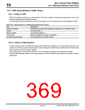
10.5 TMS (Input-Related 16-Bit Timer)
10
10.5.4 TMS Control Registers
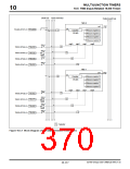
The TMS control registers are used to select TMS0/1 input events and count clock sources, as well as control
count enable. Following two TMS control registers are included:
• TMS0 Control Register (TMS0CR)
• TMS1 Control Register (TMS1CR)
TMS0 Control Register (TMS0CR)
<Address: H’0080 03CA>
<After reset: H’00>
b0
1
2
3
4
5
0
6
0
b7
TMS0SS0 TMS0SS1 TMS0SS2 TMS0SS3
TMS0CKS
TMS0CEN
0
0
0
0
0
0
b
0
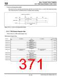
Bit Name
TMS0SS0
Function
R
R
W
W
0: External input TIN15
1: Input event bus 0
TMS0 measure 0 source select bit
1
2
3
TMS0SS1
0: External input TIN14
1: Input event bus 1
R
R
R
R
W
W
W
W
TMS0 measure 1 source select bit
TMS0SS2
0: External input TIN13
1: Input event bus 2
TMS0 measure 2 source select bit
TMS0SS3
0: External input TIN12
1: Input event bus 3
TMS0 measure 3 source select bit
4, 5
TMS0CKS
00: External input TCLK3
01: Clock bus 0
TMS0 clock source select bit
10: Clock bus 1
11: Clock bus 3
6
7
No function assigned. Fix to "0".
0
0
TMS0CEN
0: Stop count
1: Start count
R
W
TMS0 count enable bit
TMS1 Control Register (TMS1CR)
<Address: H’0080 03CB>
<After reset: H’00>
b8
9
10
11
12
13
14
0
b15
TMS1SS0 TMS1SS1 TMS1SS2 TMS1SS3
TMS1CKS
0
TMS1CEN
0
0
0
0
0
0
b
8
Bit Name
TMS1SS0
Function
R
R
W
W
0: External input TIN19
1: Input event bus 0
TMS1 measure 0 source select bit
9
TMS1SS1
0: External input TIN18
1: Input event bus 1
R
R
R
W
W
W
TMS1 measure 1 source select bit
10
11
TMS1SS2
0: External input TIN17
1: Input event bus 2
TMS1 measure 2 source select bit
TMS1SS3
0: External input TIN16
1: Input event bus 3
TMS1 measure 3 source select bit
12
13
No function assigned. Fix to "0".
0
0
TMS1CKS
0: Clock bus 0
1: Clock bus 3
R
W
TMS1 clock source select bit
14
15
No function assigned. Fix to "0".
0
0
TMS1CEN
0: Stop count
1: Start count
R
W
TMS1 count enable bit
32180 Group User’s Manual (Rev.1.0)
10-129

 RENESAS [ RENESAS TECHNOLOGY CORP ]