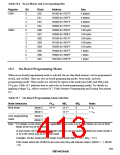
19.2.4
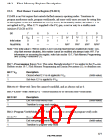
Wait-State Control Register (WSCR)
WSCR is an 8-bit readable/writable register that enables flash-memory updates to be emulated in
RAM. It also controls frequency division of clock signals supplied to the on-chip supporting
modules and insertion of wait states by the wait-state controller.
WSCR is initialized to H'08 by a reset and in hardware standby mode. It is not initialized in
software standby mode.
Bit
7
RAMS
0
6
RAM0
0
5
CKDBL
0
4
—
3
WMS1
1
2
WMS0
0
1
0
WC1
0
WC0
0
Initial value
Read/Write
0
R/W
R/W
R/W
R/W
R/W
R/W
R/W
R/W
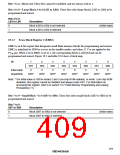
Bits 7 and 6—RAM Select and RAM0 (RAMS and RAM0): These bits are used to reassign an
area to RAM (see table 19.5). These bits are write-enabled and their initial value is 0. They are
initialized by a reset and in hardware standby mode. They are not initialized in software standby
mode.
If only one of bits 7 and 6 is set, part of the RAM area can be overlapped onto the small-block
flash memory area. In that case, access is to RAM, not flash memory, and all flash memory blocks
are write/erase-protected (emulation protect*1). In this state, the mode cannot be changed to
program or erase mode, even if the P bit or E bit in the flash memory control register (FLMCR) is
set (although verify mode can be selected). Therefore, clear both of bits 7 and 6 before
programming or erasing the flash memory area.
If both of bits 7 and 6 are set, part of the RAM area can be overlapped onto the small-block flash
memory area, but this overlapping begins only when an interrupt signal is input while 12 V is
being applied to the FVPP pin. Up until that point, flash memory is accessed. Use this setting for
interrupt handling while flash memory is being programmed or erased.*2
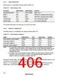
Table 19.5 RAM Area Reassignment*3
Bit 7: RAMS
Bit 6: RAM0
RAM Area
ROM Area
0
0
1
0
1
None
—
H'FC80 to H'FCFF
H'FC80 to H'FD7F
H'FC00 to H'FC7F
H'0080 to H'00FF
H'0080 to H'017F
H'0000 to H'007F
1
380

 RENESAS [ RENESAS TECHNOLOGY CORP ]