19.1.5
Input/Output Pins
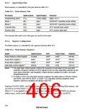
Flash memory is controlled by the pins listed in table 19.3.
Table 19.3 Flash Memory Pins
Pin Name
Abbreviation
FVPP
Input/Output
Power supply
Input
Function
Programming power
Mode 1
Apply 12.0 V
MD1
H8/3334YF operating mode setting
H8/3334YF operating mode setting
SCI1 transmit data output
SCI1 receive data input
Mode 0
MD0
Input
Transmit data
Receive data
TxD1
Output
RxD1
Input
The transmit data and receive data pins are used in boot mode.
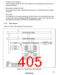
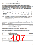
19.1.6 Register Configuration
The flash memory is controlled by the registers listed in table 19.4.
Table 19.4 Flash Memory Registers
Name
Abbreviation
FLMCR
EBR1
R/W
Initial Value
H'00*2
H'F0*2
Address
H'FF80
H'FF82
H'FF83
H'FFC2
Flash memory control register
Erase block register 1
Erase block register 2
Wait-state control register*1
R/W*2
R/W*2
R/W*2
R/W
EBR2
H'00*2
WSCR
H'08
Notes: *1 The wait-state control register controls the insertion of wait states by the wait-state
controller, frequency division of clock signals for the on-chip supporting modules by the
clock pulse generator, and emulation of flash-memory updates by RAM in on-board
programming mode.
*2 In modes 2 and 3 (on-chip flash memory enabled), the initial value is H'00 for FLMCR
and EBR2, and H'F0 for EBR1. In mode 1 (on-chip flash memory disabled), these
registers cannot be modified and always read H'FF.
Registers FLMCR, EBR1, and EBR2 are only valid when writing to or erasing flash memory, and
can only be accessed while 12 V is being applied to the FVPP pin.
When 12 V is not applied to the FVPP pin, in mode 2 addresses H'FF80 to H'FF83 are external
address space, and in mode 3 these addresses connot be modified and always read H'FF.
376

 RENESAS [ RENESAS TECHNOLOGY CORP ]