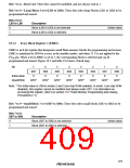
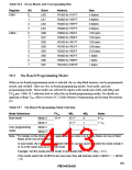
Table 19.6 Erase Blocks and Corresponding Bits
Register
Bit
0
Block
LB0
LB1
LB2
LB3
SB0
SB1
SB2
SB3
SB4
SB5
SB6
SB7
Address
Size
EBR1
H'1000 to H'1FFF
H'2000 to H'3FFF
H'4000 to H'5FFF
H'6000 to H'7FFF
H'0000 to H'007F
H'0080 to H'00FF
H'0100 to H'017F
H'0180 to H'01FF
H'0200 to H'03FF
H'0400 to H'07FF
H'0800 to H'0BFF
H'0C00 to H'0FFF
4 kbytes
8 kbytes
8 kbytes
8 kbytes
128 bytes
128 bytes
128 bytes
128 bytes
512 bytes
1 kbyte
1
2
3
EBR2
0
1
2
3
4
5
6
1 kbyte
7
1 kbyte
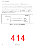
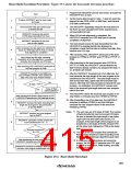
19.3
On-Board Programming Modes
When an on-board programming mode is selected, the on-chip flash memory can be programmed,
erased, and verified. There are two on-board programming modes: boot mode, and user
programming mode. These modes are selected by inputs at the mode pins (MD1 and MD0) and
FVPP pin. Table 19.7 indicates how to select the on-board programming modes. For details on
applying voltage VPP, refer to section 19.7, Flash Memory Programming and Erasing Precautions
(5).
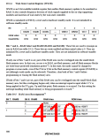
Table 19.7 On-Board Programming Mode Selection
Mode Selections
FVPP
MD1
12 V*
12 V*
1
MD0
0
Notes
0: VIL
1: VIH
Boot mode
Mode 2
Mode 3
Mode 2
Mode 3
12 V*
1
User programming
mode
0
1
1
Note: * For details on the timing of 12 V application, see notes 6 to 8 in the Notes on Use of Boot
Mode at the end of this section.
In boot mode, the mode control register (MDCR) can be used to monitor the mode (mode 2
or 3) in the same way as in normal mode.
Example: Set the mode pins for mode 2 boot mode (MD1 = 12 V, MD0 = 0 V).
If the mode select bits of MDCR are now read, they will indicate mode 2 (MDS1 = 1, MDS0
= 0).
383

 RENESAS [ RENESAS TECHNOLOGY CORP ]