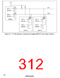
13.1.3
Input/Output Pins
Table 13.1 summarizes the input/output pins used by the I2C bus interface.
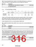
Table 13.1 I2C Bus Interface
Name
Abbreviation
SCL
I/O
Function
Serial clock
Serial data
Input/output
Input/output
Serial clock input/output
Serial data input/output
SDA
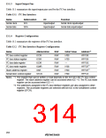
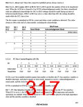
13.1.4
Register Configuration
Table 13.2 summarizes the registers of the I2C bus interface.
Table 13.2 I2C Bus Interface Register Configuration
Name
Abbreviation
ICCR
R/W
R/W
R/W
R/W
R/W
R/W
R/W
Initial Value
H'00
Address*2
H'FFD8
I2C bus control register
I2C bus status register
I2C bus data register
I2C bus mode register
Slave address register
Serial timer control register
ICSR
H'30
H'FFD9
ICDR
—
H'FFDE
H'FFDF*1
H'FFDF*1
H'FFC3
ICMR
H'38
SAR
H'00
STCR
H'00
Notes: *1 The register that can be written or read depends on the ICE bit in the I2C bus control
register. The slave address register can be accessed when ICE = 0. The I2C bus mode
register can be accessed when ICE = 1.
*2 The addresses assigned to the I2C bus interface registers are also assigned to other
registers. The accessible registers are selected with bit IICE in the serial/timer control
register (STCR).
284

 RENESAS [ RENESAS TECHNOLOGY CORP ]