Section 13 I2C Bus Interface (H8/3337 Series Only)
[Option]
An I2C bus interface is available as an option. Observe the following notes when using this option.
•
For mask-ROM versions, the Y in the part number becomes a W in products in which this
optional function is used.
Examples: HD6433337WF, HD6433334WF
13.1
Overview
The I2C bus interface conforms to and provides a subset of the Philips I2C bus (inter-IC bus)
interface functions. The register configuration that controls the I2C bus differs partly from the
Philips configuration, however.
The I2C bus interface uses only one data line (SDA) and one clock line (SCL) to transfer data, so it
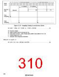
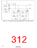
can save board and connector space. Figure 13.1 shows typical I2C bus interface connections.
13.1.1
Features
•
•
•
•
•
•
•
Conforms to Philips I2C bus interface
Start and stop conditions generated automatically
Selectable acknowledge output level when receiving
Auto-loading of acknowledge bit when transmitting
Selection of eight internal clocks (in master mode)
Selection of acknowledgement mode, or serial mode without acknowledge bit
Wait function: a wait can be inserted in acknowledgement mode by holding the SCL pin low
after a data transfer, before acknowledgement of the transfer.
•
Three interrupt sources
Data transfer end
In slave receive mode: slave address matched, or general call address received
In master transmit mode: bus arbitration lost
Direct bus drive (with pins SCL and SDA)
•
•
The P86/SCK1/SCL pin and the P97/WAIT/SDA pin are NMOS outputs only when the bus
drive function is selected
281

 RENESAS [ RENESAS TECHNOLOGY CORP ]