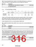
Bits 5 to 3—Reserved: These bits cannot be modified and are always read as 1.
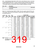
Bits 2 to 0—Bit Counter (BC2 to BC0): BC2 to BC0 specify the number of bits to be transferred
next. When the ACK bit is cleared to 0 in ICCR (acknowledgement mode), the data is transferred
with one additional acknowledge bit. BC2 to BC0 settings should be made during an interval
between transfer frames. If BC2 to BC0 are set to a value other than 000, the setting should be
made while the SCL line is low.
The bit counter is initialized to 000 by a reset and when a start condition is detected. The value
returns to 000 at the end of a data transfer, including the acknowledge.
Bits/Frame
Bit 2:
BC2
Bit 1:
BC1
Bit 0:
BC0
Serial Mode
Acknowledgement Mode
0
0
1
0
1
0
1
0
1
0
1
0
1
8
1
2
3
4
5
6
7
9
2
3
4
5
6
7
8
(Initial value)
1
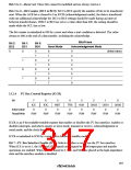
13.2.4
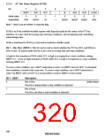
I2C Bus Control Register (ICCR)
Bit
7
6
5
4
3
2
CKS2
0
1
0
ICE
0
IEIC
0
MST
0
TRS
0
ACK
0
CKS1
0
CKS0
0
Initial value
Read/Write
R/W
R/W
R/W
R/W
R/W
R/W
R/W
R/W
ICCR is an 8-bit readable/writable register that enables or disables the I2C bus interface, enables or
disables interrupts, and selects master or slave mode, transmit or receive, acknowledgement or
serial mode, and the clock frequency.
ICCR is initialized to H'00 by a reset and in hardware standby mode.
Bit 7—I2C Bus Interface Enable (ICE): Selects whether or not to use the I2C bus interface.
When ICE is set to 1, the SCL and SDA signals are assigned to input/output pins and transfer
operations are enabled. When ICE is cleared to 0, SCL and SDA are placed in the high-impedance
state and the interface module is disabled.
287

 RENESAS [ RENESAS TECHNOLOGY CORP ]