8.2.3
Input Capture Registers A to D (ICRA to ICRD)
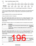
Bit
15 14 13 12 11 10
9
8
7
6
5
4
3
2
1
0
Initial value
Read/Write
0
0
0
0
0
0
0
0
0
0
0
0
0
0
0
0
R
R
R
R
R
R
R
R
R
R
R
R
R
R
R
R
There are four input capture registers A to D, each of which is a 16-bit read-only register.
When the rising or falling edge of the signal at an input capture pin (FTIA to FTID) is detected,
the current FRC value is copied to the corresponding input capture register (ICRA to ICRD).* At
the same time, the corresponding input capture flag (ICFA to ICFD) in the timer control/status
register (TCSR) is set to 1. The input capture edge is selected by the input edge select bits
(IEDGA to IEDGD) in the timer control register (TCR).
Note: * The FRC contents are transferred to the input capture register regardless of the value of the
input capture flag (ICFA/B/C/D).
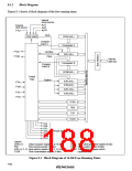
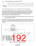
Input capture can be buffered by using the input capture registers in pairs. When the BUFEA bit in
TCR is set to 1, ICRC is used as a buffer register for ICRA as shown in figure 8.2. When an FTIA
input is received, the old ICRA contents are moved into ICRC, and the new FRC count is copied
into ICRA.
BUFEA
IEDGA IEDGC
Edge detect and
capture signal
generating circuit
FTIA
ICRC
ICRA
FRC
BUFEA: Buffer enable A
IEDGA: Input edge select A
IEDGC: Input edge select C
ICRC:
ICRA:
FRC:
Input capture register C
Input capture register A
Free-running counter
Figure 8.2 Input Capture Buffering (Example)
162

 RENESAS [ RENESAS TECHNOLOGY CORP ]