Section 17 I2C Bus Interface 2 (IIC2)
17.4.6
Clock Synchronous Serial Format
This module can be operated with the clock synchronous serial format, by setting the FS bit in
SAR to 1. When the MST bit in ICCR1 is 1, the transfer clock output from SCL is selected. When
MST is 0, the external clock input is selected.
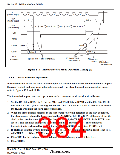
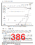
Data Transfer Format
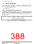
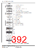
Figure 17.13 shows the clock synchronous serial transfer format.
The transfer data is output from the rise to the fall of the SCL clock, and the data at the rising edge
of the SCL clock is guaranteed. The MLS bit in ICMR sets the order of data transfer, in either the
MSB first or LSB first. The output level of SDA can be changed during the transfer wait, by the
SDAO bit in ICCR2.
SCL
Bit 0 Bit 1 Bit 2 Bit 3 Bit 4 Bit 5 Bit 6 Bit 7
SDA
Figure 17.13 Clock Synchronous Serial Transfer Format
Rev. 3.00 Sep. 10, 2007 Page 354 of 528
REJ09B0216-0300

 RENESAS [ RENESAS TECHNOLOGY CORP ]