Section 17 I2C Bus Interface 2 (IIC2)
17.4.7
Noise Filter
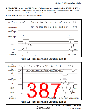
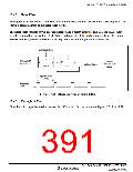
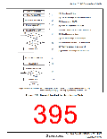
The signal levels on the SCL and SDA pins are internally latched via the noise filter. Figure 17.16
shows a block diagram of the noise filter circuit.
The noise filter consists of two cascaded latches and a match detector. The SCL (or SDA) input
signal is sampled on the system clock. When both outputs of the latches match, its level is output
to other blocks by the match detector. If they do not match, the previous value is held.
Sampling clock
C
C
SCL or SDA
input signal
Internal
SCL or SDA
signal
D
Q
D
Q
Match detector
Latch
Latch
System clock
cycle
Sampling
clock
Figure 17.16 Block Diagram of Noise Filter
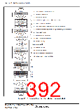
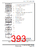
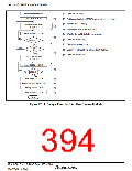
17.4.8
Example of Use
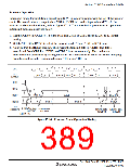
Flowcharts in respective modes that use the I2C bus interface are shown in figures 17.17 to 17.20.
Rev. 3.00 Sep. 10, 2007 Page 357 of 528
REJ09B0216-0300

 RENESAS [ RENESAS TECHNOLOGY CORP ]