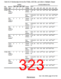
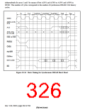
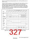
Figure 10.15 shows the burst read timing when RCD is set to 1, A3W1 and A3W0 are set to 10,
and TPC is set to 1.
The BS cycle, which is asserted for one cycle at the start of a bus cycle for normal access space, is
asserted in each of cycles Td1–Td4 in a synchronous DRAM cycle. When a burst read is
performed, the address is updated each time CAS is asserted. As the unit of burst transfer is 16
bytes, address updating is performed for A3 and A2 only (when the bus width is 16 bits, address
updating is performed for A3, A2, and A1). The order of access is as follows: in a fill operation in
the event of a cache miss, the missed data is read first, then 16-byte boundary data including the
missed data is read in wraparound mode.
Tr
Trw
Tc1
Tc2 Tc3/Td1 Tc4/Td2 Td3
Td4
Tpc
CKIO
A25 to A16,
A13
A12
A15, A14,
A11 to A0
CS2 or CS3
RAS3x
CASx
RD/WR
DQMxx
D31 to D0
BS
Figure 10.15 Synchronous DRAM Burst Read Wait Specification Timing
Rev. 5.00, 09/03, page 283 of 760

 RENESAS [ RENESAS TECHNOLOGY CORP ]