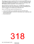
64M synchronous DRAM
(1M × 16 bit × 4 bank)
SH7709S
A13
A12
A11
A14
A13
A12
A0
A1
CLK
CKE
CS
CKIO
CKE
CSn
RAS
CAS
WE
RAS3x
CASx
RD/WR
D15
DQ15
DQ0
DQMU
DQML
D0
DQMLU
DQMLL
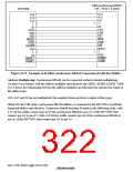
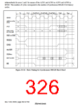
Figure 10.13 Example of 64-Mbit Synchronous DRAM Connection (16-Bit Bus Width)
Address Multiplexing: Synchronous DRAM can be connected without external multiplexing
circuitry in accordance with the address multiplex specification bits AMX2-AMX0 in MCR. Table
10.13 shows the relationship between the address multiplex specification bits and the bits output at
the address pins.
A25–A17 and A0 are not multiplexed; the original values are always output at these pins.
When A0, the LSB of the synchronous DRAM address, is connected to the SH7709S, it performs
longword address specification. Connection should therefore be made in the following order: with
a 32-bit bus width, connect pin A0 of the synchronous DRAM to pin A2 of the SH7709S, then
connect pin A1 to pin A3; with a 16-bit bus width, connect pin A0 of the synchronous DRAM to
pin A1 of the SH7709S, then connect pin A1 to pin A2.
Rev. 5.00, 09/03, page 278 of 760

 RENESAS [ RENESAS TECHNOLOGY CORP ]