10.3.4 Synchronous DRAM Interface
Synchronous DRAM Direct Connection: Since synchronous DRAM can be selected by the CS
signal, physical space areas 2 and 3 can be connected using RAS and other control signals in
common. If the memory type bits (DRAMTP2–0) in BCR1 are set to 010, area 2 is ordinary
memory space and area 3 is synchronous DRAM space; if set to 011, areas 2 and 3 are both
synchronous DRAM space. Note, however, that synchronous DRAM must not be accessed when
clock ratio Iφ:Bφ = 1:1.
With the SH7709S, burst length 1 burst read/single write mode is supported as the synchronous
DRAM operating mode. A data bus width of 16 or 32 bits can be selected. A 16-bit burst transfer
is performed in a cache fill/write-back cycle, and only one access is performed in a write-through
area write or a non-cacheable area read/write.
The control signals for direct connection of synchronous DRAM are RAS3L, RAS3U, CASL,
CASU, RD/WR, CS2 or CS3, DQMUU, DQMUL, DQMLU, DQMLL, and CKE. All the signals
other than CS2 and CS3 are common to all areas, and signals other than CKE are valid and fetched
to the synchronous DRAM only when CS2 or CS3 is asserted. Synchronous DRAM can therefore
be connected in parallel to a number of areas. CKE is negated (low) only when self-refreshing is
performed, and is always asserted (high) at other times.
In the refresh cycle and mode-register write cycle, RAS3U and RAS3L or CASU and CASL are
output.
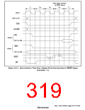
Commands for synchronous DRAM are specified by RAS3L, RAS3U, CASL, CASU, RD/WR,
and special address signals. The commands are NOP, auto-refresh (REF), self-refresh (SELF),
precharge all banks (PALL), row address strobe bank active (ACTV), read (READ), read with
precharge (READA), write (WRIT), write with precharge (WRITA), and mode register write
(MRS).
Byte specification is performed by DQMUU, DQMUL, DQMLU, and DQMLL. A read/write is
performed for the byte for which the corresponding DQM is low. In big-endian mode, DQMUU
specifies an access to address 4n, and DQMLL specifies an access to address 4n + 3. In little-
endian mode, DQMUU specifies an access to address 4n + 3, and DQMLL specifies an access to
address 4n.
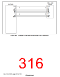
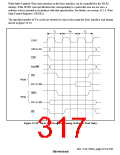
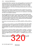
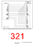
Figures 10.12 and 10.13 show examples of the connection of two 1M × 16-bit × 4-bank
synchronous DRAMs and one 1M × 16-bit × 4-bank synchronous DRAM, respectively.
Rev. 5.00, 09/03, page 276 of 760

 RENESAS [ RENESAS TECHNOLOGY CORP ]